
Connect two separate power sources the gate and drain pins
EGRE 306 – Introduction to Microelectronics
Using Multisim, you will first measure the I-V characteristics of an n-channel MOSFET so that you can predict the transistor’s behavior. Then, you will take data to use the transistor as a voltage-controlled resistor.
Set-Up
To measure the threshold voltage, you will apply a large VDS voltage (10V) and slowly increase the gate voltage until you obtain a current. Remember that if VGS < Vt, then the transistor will be in the cutoff region and “no” current will flow.
Continue to increase VGS and measure and plot the ID vs. VGS graph for your transistor. Your resulting graph should resemble the figure below. Do not exceed 200mA.
Now, you will take data to help you calibrate your voltage-controlled resistor.
Set vDS to a small value (~50mV).
ID = 0.4mA at VGS=4V
vDS = 0.1V ID = 0.5mA at VGS=3V
For VGS = 4V The drain current increased 0.7mA when the drain voltage
increased by 0.05V. The channel resistance at VGS = 4V is:
Using your results, determine the MOSFET transconductance value (kn) for your transistor (calculate it for each of your ten data points).
Determine the correct bias conditions (VGS) so that your transistor has a resistance of 110 Ohms.
Part II Data
kn = ____________
EGRE 306 – Introduction to Microelectronics
Part II - DC Biasing of MOSFET
Connect two separate power supplies to the Drain and Gate of your MOSFET. Apply a large VDS voltage (5V).
Connect the Source to ground and use the ammeter to measure the drain current (between the VDD source and the drain of the transistor).
Using the data from steps 3, 4, 5, 6 and
ID = 0.5 kn (VGS1 – Vt)2 4ID = 0.5 kn (VGS2 – Vt)2
Vt = ________________ kn = ________________
Q1: For all of these measurements, what region of operation is the transistor operating in?
2. Find (calculate) RG1 and RD so that there will be a drain
current of ~20mA and VDS ~VDD/2
Analysis Hints:
Assume the transistor is operating in the saturation region.
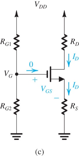 Part III – Another
DC Biasing Circuit for MOSFET
Part III – Another
DC Biasing Circuit for MOSFET
1. Build the circuit on the right, using your
measure VD, VS, and ID.
Analysis Hints:
Q3: What are pros/cons of this biasing circuit?
Lab Report (Individually done, One per PERSON)
1. Cover Page (As seen on previous templates, include: name, class, title, section, date, partner (if you have one), honor pledge - signed, etc.)
2. Introduction to the lab: Explain what the purpose of this lab was and a brief description of the purpose for each part of the lab you completed (max of 2 paragraphs).
5. Conclusion: This is where you write a summary of the experiment, including answers to all of the questions that were included in the lab handout.
To Be Included:
determined the threshold voltage and MOSFET transconductance parameters for your transistor. (This will be a lengthy answer)
3. Schematic diagram of your Part II circuit (using Multisim). Include voltmeter/ammeter
items that you should include in the appropriate areas are:
Description of HOW you determined Vt for your transistor.
voltmeter/ammeter where you measured voltage and current.
7. Part III calculations, showing how you determined RS and RG1 that satisfy the given