
Flash patch and breakpoint unit
This page intentionally left blank
Computer organization and arChiteCture
With Foreword by
Chris Jesshope
Professor (emeritus) University of Amsterdam

Director of Field Marketing: Demetrius Hall
Product Marketing Manager: Bram van Kempen Marketing Assistant: Jon Bryant
Cover Designer: Marta Samsel
Cover Art: © anderm / Fotolia
Full-Service Project Management:
Mahalatchoumy Saravanan, Jouve India
Printer/Binder: Edwards Brothers Malloy
Cover Printer: Lehigh-Phoenix Color/Hagerstown Typeface: Times Ten LT Std 10/12Senior Specialist, Program Planning and Support:
Maura Zaldivar-GarciaPearson Education North Asia Ltd., Hong Kong
Pearson Education Canada, Inc., Toronto
Pearson Education de Mexico, S.A. de C.V.Pearson Education–Japan, Tokyo
Pearson Education Malaysia, Pte. Ltd.pages cm
Includes bibliographical references and index.ISBN 978-0-13-410161-3 — ISBN 0-13-410161-8 1. Computer organization. 2. Computer architecture. I. Title.
This page intentionally left blank

PART ONE INTRODUCTION 1
Chapter 1 Basic Concepts and Computer Evolution 1
1.5 Embedded Systems 29
1.6 Arm Architecture 33
2.2 Multicore, Mics, and GPGPUs 52
2.3 Two Laws that Provide Insight: Ahmdahl’s Law and Little’s Law 53
PART TWO THE COMPUTER SYSTEM 80
Chapter 3 A Top- Level View of Computer Function and Interconnection 80
3.5 Point- to- Point Interconnect 102
3.6 PCI Express 107
4.3 Elements of Cache Design 131
4.4 Pentium 4 Cache Organization 149
Chapter 5 Internal Memory 165
5.1 Semiconductor Main Memory 166
5.6 Key Terms, Review Questions, and Problems 190
Chapter 6 External Memory 194
6.5 Magnetic Tape 222
6.6 Key Terms, Review Questions, and Problems 224
7.4 Interrupt- Driven I/O 239
7.5 Direct Memory Access 248
7.10 Key Terms, Review Questions, and Problems 270
Chapter 8 Operating System Support 275
8.5 Arm Memory Management 309
8.6 Key Terms, Review Questions, and Problems 314
9.3 The Binary System 321
9.4 Converting Between Binary and Decimal 321
10.2 Integer Representation 330
10.3 Integer Arithmetic 335
Chapter 11 Digital Logic 372
11.1 Boolean Algebra 373
11.6 Key Terms and Problems 409
PART FOUR THE CENTRAL PROCESSING UNIT 412
12.4 Types of Operations 425
12.5 Intel x86 and ARM Operation Types 438
13.2 x86 and ARM Addressing Modes 463
13.3 Instruction Formats 469
14.1 Processor Organization 489
14.2 Register Organization 491
14.7 Key Terms, Review Questions, and Problems 530
Chapter 15 Reduced Instruction Set Computers 535
15.5 RISC Pipelining 555
15.6 MIPS R4000 559
Chapter 16 Instruction- Level Parallelism and Superscalar Processors 575
16.1 Overview 576
16.6 Key Terms, Review Questions, and Problems 608
PART FIVE PARALLEL ORGANIZATION 613
17.4 Multithreading and Chip Multiprocessors 628
17.5 Clusters 633
18.1 Hardware Performance Issues 657
18.2 Software Performance Issues 660
18.7 IBM zEnterprise EC12 Mainframe 682
18.8 Key Terms, Review Questions, and Problems 685
19.4 Intel’s Gen8 GPU 701
19.5 When to Use a GPU as a Coprocessor 704
20.2 Control of the Processor 714
20.3 Hardwired Implementation 724
Contents xi
21.3 Microinstruction Execution 745
A.2 Research Projects 771
A.3 Simulation Projects 771
Appendix B Assembly Language and Related Topics 774
B.1 Assembly Language 775
Index 809
Credits 833
|
|---|
at the front of this book.
This page intentionally left blank
Throughout the 1980s and early 1990s research flourished in this field and there was a great deal of innovation, much of which came to market through university start- ups. Iron-ically however, it was the same technology that reversed this trend. Diversity was gradually replaced with a near monoculture in computer systems with advances in just a few instruc-tion set architectures. Moore’s law, a self- fulfilling prediction that became an industry guide-line, meant that basic device speeds and integration densities both grew exponentially, with the latter doubling every 18 months of so. The speed increase was the proverbial free lunch for computer architects and the integration levels allowed more complexity and innovation at the micro- architecture level. The free lunch of course did have a cost, that being the expo-nential growth of capital investment required to fulfill Moore’s law, which once again limited the access to state- of- the- art technologies. Moreover, most users found it easier to wait for the next generation of mainstream processor than to invest in the innovations in parallel computers, with their pitfalls and difficulties. The exceptions to this were the few large insti-tutions requiring ultimate performance; two topical examples being large- scale scientific simulation such as climate modeling and also in our security services for code breaking. For
xiii
These are just some of the questions facing us today. To answer these questions and more requires a sound foundation in computer organization and architecture, and this book by William Stallings provides a very timely and comprehensive foundation. It gives a com-plete introduction to the basics required, tackling what can be quite complex topics with apparent simplicity. Moreover, it deals with the more recent developments in this field, where innovation has in the past, and is, currently taking place. Examples are in superscalar issue and in explicitly parallel multicores. What is more, this latest edition includes two very recent topics in the design and use of GPUs for general- purpose use and the latest trends in cloud computing, both of which have become mainstream only recently. The book makes good use of examples throughout to highlight the theoretical issues covered, and most of these examples are drawn from developments in the two most widely used ISAs, namely the x86 and ARM. To reiterate, this book is complete and is a pleasure to read and hopefully will kick- start more young researchers down the same path that I have enjoyed over the last 40 years!

■ GPGPU [ General- Purpose Computing on Graphics Processing Units (GPUs)]: One of the most important new developments in recent years has been the broad adoption of GPGPUs to work in coordination with traditional CPUs to handle a wide range of applications involving large arrays of data. A new chapter is devoted to the topic of GPGPUs.
■ Heterogeneous multicore processors: The latest development in multicore architecture is the heterogeneous multicore processor. A new section in the chapter on multicore processors surveys the various types of heterogeneous multicore processors.
xv
xvi PreFACe
■ Homework problems: The number of supplemental homework problems, with solu- tions, available for student practice has been expanded.
SUPPORT OF ACM/IEEE COMPUTER SCIENCE CURRICULA 2013
|
Textbook Coverage | |
|---|---|---|
|
||
|
||
|
||
|
||
|
||
|
xviii PreFACe
The subtitle suggests the theme and the approach taken in this book. It has always been important to design computer systems to achieve high performance, but never has this requirement been stronger or more difficult to satisfy than today. All of the basic per-formance characteristics of computer systems, including processor speed, memory speed, memory capacity, and interconnection data rates, are increasing rapidly. Moreover, they are increasing at different rates. This makes it difficult to design a balanced system that maxi-mizes the performance and utilization of all elements. Thus, computer design increasingly becomes a game of changing the structure or function in one area to compensate for a per-formance mismatch in another area. We will see this game played out in numerous design decisions throughout the book.
A computer system, like any system, consists of an interrelated set of components. The system is best characterized in terms of structure— the way in which components are interconnected, and function— the operation of the individual components. Furthermore, a computer’s organization is hierarchical. Each major component can be further described by decomposing it into its major subcomponents and describing their structure and function. For clarity and ease of understanding, this hierarchical organization is described in this book from the top down:
PreFACe xix
Throughout the discussion, aspects of the system are viewed from the points of view of both architecture (those attributes of a system visible to a machine language programmer) and organization (the operational units and their interconnections that realize the architecture).
Many, but by no means all, of the examples in this book are drawn from these two computer families. Numerous other systems, both contemporary and historical, provide examples of important computer architecture design features.
PLAN OF THE TEXT
■ The central processing unit
■ Parallel organization, including multicore
xx PreFACe
book’s Companion Web site at WilliamStallings.com/ComputerOrganization. To gain access to the IRC, please contact your local Pearson sales representative via pearsonhighered.com/ educator/replocator/requestSalesRep.page or call Pearson Faculty Services at 1-800-526-0485. The IRC provides the following materials:
■ Test bank: A chapter- by- chapter set of questions.
■ Sample syllabuses: The text contains more material than can be conveniently covered in one semester. Accordingly, instructors are provided with several sample syllabuses that guide the use of the text within limited time. These samples are based on real- world experience by professors with the first edition.
errata sheet for the book.
PreFACe xxi
 |
|
|---|
■ Research projects: A series of research assignments that instruct the student to research a particular topic on the Internet and write a report.
■ Simulation projects: The IRC provides support for the use of the two simulation pack-ages: SimpleScalar can be used to explore computer organization and architecture design issues. SMPCache provides a powerful educational tool for examining cache design issues for symmetric multiprocessors.
This diverse set of projects and other student exercises enables the instructor to use the book as one component in a rich and varied learning experience and to tailor a course plan to meet the specific needs of the instructor and students. See Appendix A in this book for details.
INTERACTIVE SIMULATIONS
ACKNOWLEDGMENTS
This new edition has benefited from review by a number of people, who gave generously of their time and expertise. The following professors and instructors reviewed all or a large part of the manuscript: Molisa Derk (Dickinson State University), Yaohang Li (Old Domin-ion University), Dwayne Ockel (Regis University), Nelson Luiz Passos (Midwestern State University), Mohammad Abdus Salam (Southern University), and Vladimir Zwass (Fair-leigh Dickinson University).
Todd Bezenek of the University of Wisconsin and James Stine of Lehigh University prepared the SimpleScalar problems in the instructor’s manual, and Todd also authored the SimpleScalar User’s Guide.
Finally, I would like to thank the many people responsible for the publication of the book, all of whom did their usual excellent job. This includes the staff at Pearson, par-ticularly my editor Tracy Johnson, her assistant Kelsey Loanes, program manager Carole Snyder, and production manager Bob Engelhardt. I also thank Mahalatchoumy Saravanan and the production staff at Jouve India for another excellent and rapid job. Thanks also to the marketing and sales staffs at Pearson, without whose efforts this book would not be in front of you.
Dr. Stallings holds a PhD from MIT in computer science and a BS from Notre Dame in electrical engineering.
xxiii
Basic conceptsand computer evolution
1.1 Organization and Architecture
1.6 ARM Architecture
ARM Evolution
Instruction Set Architecture
ARM Products1.7 Cloud Computing
Basic Concepts
Cloud Services
In describing computers, a distinction is often made between computer architec-ture and computer organization. Although it is difficult to give precise definitions for these terms, a consensus exists about the general areas covered by each. For example, see [VRAN80], [SIEW82], and [BELL78a]; an interesting alternative view is presented in [REDD76].
Computer architecture refers to those attributes of a system visible to a pro-grammer or, put another way, those attributes that have a direct impact on the logical execution of a program. A term that is often used interchangeably with com-puter architecture is instruction set architecture (ISA). The ISA defines instruction formats, instruction opcodes, registers, instruction and data memory; the effect of executed instructions on the registers and memory; and an algorithm for control-ling instruction execution. Computer organization refers to the operational units and their interconnections that realize the architectural specifications. Examples of architectural attributes include the instruction set, the number of bits used to repre-sent various data types (e.g., numbers, characters), I/O mechanisms, and techniques for addressing memory. Organizational attributes include those hardware details transparent to the programmer, such as control signals; interfaces between the com-puter and peripherals; and the memory technology used.
In a class of computers called microcomputers, the relationship between archi-tecture and organization is very close. Changes in technology not only influence organization but also result in the introduction of more powerful and more complex architectures. Generally, there is less of a requirement for generation- to- generation compatibility for these smaller machines. Thus, there is more interplay between organizational and architectural design decisions. An intriguing example of this is the reduced instruction set computer (RISC), which we examine in Chapter 15.
This book examines both computer organization and computer architecture. The emphasis is perhaps more on the side of organization. However, because a computer organization must be designed to implement a particular architectural specification, a thorough treatment of organization requires a detailed examination of architecture as well.
■ Function: The operation of each individual component as part of the structure.
In terms of description, we have two choices: starting at the bottom and build-ing up to a complete description, or beginning with a top view and decomposing the system into its subparts. Evidence from a number of fields suggests that the top- down approach is the clearest and most effective [WEIN75].
Both the structure and functioning of a computer are, in essence, simple. In general terms, there are only four basic functions that a computer can perform:
■ Data processing: Data may take a wide variety of forms, and the range of pro-cessing requirements is broad. However, we shall see that there are only a few fundamental methods or types of data processing.
There is remarkably little shaping of computer structure to fit the function to be performed. At the root of this lies the general- purpose nature of computers, in which all the functional specialization occurs at the time of programming and not at the time of design.
Structure
1.2 / struCture and FunCtion 5
CPU
| Registers | ALU |
|---|
Internal
busControl
memoryFigure 1.1 The Computer: Top- Level Structure
Each of these components will be examined in some detail in Part Two. How-ever, for our purposes, the most interesting and in some ways the most complex component is the CPU. Its major structural components are as follows:
■ Control unit: Controls the operation of the CPU and hence the computer.
multicorecomputerstructure As was mentioned, contemporary computers generally have multiple processors. When these processors all reside on a single chip, the term multicore computer is used, and each processing unit (consisting of a control unit, ALU, registers, and perhaps cache) is called a core. To clarify the terminology, this text will use the following definitions.
■ Central processing unit (CPU): That portion of a computer that fetches and executes instructions. It consists of an ALU, a control unit, and registers. In a system with a single processing unit, it is often simply referred to as a processor.
1.2 / struCture and FunCtion 7
I/O chips chip
PROCESSOR CHIP
Arithmetic
Instruction Load/
and logic
logic store logic
unit (ALU)L1 I-cache L1 data cache
Figure 1.2 shows a processor chip that contains eight cores and an L3 cache. Not shown is the logic required to control operations between the cores and the cache and between the cores and the external circuitry on the motherboard. The figure indicates that the L3 cache occupies two distinct portions of the chip surface. However, typically, all cores have access to the entire L3 cache via the aforemen-tioned control circuits. The processor chip shown in Figure 1.2 does not represent any specific product, but provides a general idea of how such chips are laid out.
Next, we zoom in on the structure of a single core, which occupies a portion of the processor chip. In general terms, the functional elements of a core are:
Keep in mind that this representation of the layout of the core is only intended to give a general idea of internal core structure. In a given product, the functional elements may not be laid out as the three distinct elements shown in Figure 1.2, especially if some or all of these functions are implemented as part of a micropro-grammed control unit.
examples It will be instructive to look at some real- world examples that illustrate the hierarchical structure of computers. Figure 1.3 is a photograph of the motherboard for a computer built around two Intel Quad- Core Xeon processor chips. Many of the elements labeled on the photograph are discussed subsequently in this book. Here, we mention the most important, in addition to the processor sockets:
1.2 / struCture and FunCtion 9
Intel® 3420
2x USB 2.0
Internal
2x USB 2.0
External
| Power & Backplane I/O | PCI Express® | PCI Express® |
|
|---|---|---|---|
| Connector C | Connector B | Connector A |
Figure 1.3 Motherboard with Two Intel Quad- Core Xeon Processors Source: Chassis Plans, www.chassis-plans.com
Going down one level deeper, we examine the internal structure of a single core, as shown in the photograph of Figure 1.5. Keep in mind that this is a portion of the silicon surface area making up a single- processor chip. The main sub- areas within this core area are the following:
■ ISU (instruction sequence unit): Determines the sequence in which instructions are executed in what is referred to as a superscalar architecture (Chapter 16).
Figure 1.5 zEnterprise EC12 Core layout Source: IBM zEnterprise EC12 Technical Guide, December 2013, SG24-8049-01. IBM, Reprinted by
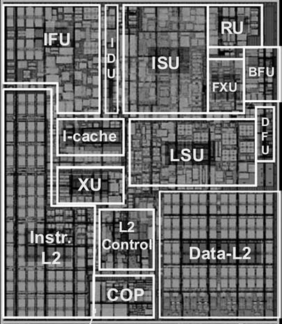
■ FXU ( fixed- point unit): The FXU executes fixed- point arithmetic operations.
■ BFU (binary floating- point unit): The BFU handles all binary and hexadeci-mal floating- point operations, as well as fixed- point multiplication operations.
■ COP (dedicated co- processor): The COP is responsible for data compression and encryption functions for each core.
■ I- cache: This is a 64-kB L1 instruction cache, allowing the IFU to prefetch instructions before they are needed.
1.3 a BrieF hiStOry OF cOmputerS2
In this section, we provide a brief overview of the history of the development of computers. This history is interesting in itself, but more importantly, provides a basic introduction to many important concepts that we deal with throughout the book.
■ A main memory, which stores both data and instructions5
■ An arithmetic and logic unit (ALU) capable of operating on binary data
12 Chapter 1 / BasiC ConCepts and Computer evolution
Central processing unit (CPU)
Instructions
and data
| Main | MAR | IR | |
|---|---|---|---|
| memory |
|
(M)
Addresses
Figure 1.6 IAS Structure
1.3 / a BrieF history oF Computers 13
It must be observed, however, that while this principle as such is probably sound, the specific way in which it is realized requires close scrutiny. At any rate a central arithmetical part of the device will probably have to exist, and this constitutes the first specific part: CA.
2.6 The three specific parts CA, CC (together C), and M cor-respond to the associative neurons in the human nervous system. It remains to discuss the equivalents of the sensory or afferent and the motor or efferent neurons. These are the input and output organs of the device.
The device must be endowed with the ability to maintain input and output (sensory and motor) contact with some specific medium of this type. The medium will be called the outside record-ing medium of the device: R.
are changed in the following to conform more closely to modern usage; the exam-ples accompanying this discussion are based on that latter text.
The memory of the IAS consists of 4,096 storage locations, called words, of 40 binary digits (bits) each.6 Both data and instructions are stored there. Numbers are represented in binary form, and each instruction is a binary code. Figure 1.7 illustrates these formats. Each number is represented by a sign bit and a 39-bit value. A word may alternatively contain two 20-bit instructions, with each instruction consisting of an 8-bit operation code (opcode) specifying the operation to be performed and a 12-bit address designating one of the words in memory (numbered from 0 to 999).
■ Instruction buffer register (IBR): Employed to hold temporarily the right- hand instruction from a word in memory.
■ Program counter (PC): Contains the address of the next instruction pair to be fetched from memory.
left instruction (20 bits) right instruction (20 bits)

6There is no universal definition of the term word. In general, a word is an ordered set of bytes or bits that is the normal unit in which information may be stored, transmitted, or operated on within a given computer. Typically, if a processor has a fixed- length instruction set, then the instruction length equals the word length.
Start
| Fetch | Yes | Is next | No | MAR PC |
|
|||
|---|---|---|---|---|---|---|---|---|
| instruction in IBR? | ||||||||
| cycle | MBR M(MAR) | |||||||
| required | ||||||||
| IR MBR (20:27) | No | Left | Yes | |||||
| instruction | ||||||||
| MAR IBR (8:19) | MAR MBR (28:39) | |||||||
| required? | ||||||||
PC PC + 1
Decode instruction in IR
M(X) = contents of memory location whose address is X (i:j) = bits i through j
Figure 1.8 Partial Flowchart of IAS Operation
■ Data transfer: Move data between memory and ALU registers or between two ALU registers.
■ Unconditional branch: Normally, the control unit executes instructions in sequence from memory. This sequence can be changed by a branch instruc-tion, which facilitates repetitive operations.
|
||||||||||||||||||||||
instruction from right half of M(X) |
||||||||||||||||||||||
|
||||||||||||||||||||||
1.3 / a BrieF history oF Computers 17
■ Conditional branch: The branch can be made dependent on a condition, thus allowing decision points.
The Second Generation: Transistors
The first major change in the electronic computer came with the replacement of the vacuum tube by the transistor. The transistor, which is smaller, cheaper, and gener-ates less heat than a vacuum tube, can be used in the same way as a vacuum tube to construct computers. Unlike the vacuum tube, which requires wires, metal plates, a glass capsule, and a vacuum, the transistor is a solid- state device, made from silicon.
|
Also, over the lifetime of this series of computers, the relative speed of the CPU increased by a factor of 50. Speed improvements are achieved by improved electronics (e.g., a transistor implementation is faster than a vacuum tube imple-mentation) and more complex circuitry. For example, the IBM 7094 includes an Instruction Backup Register, used to buffer the next instruction. The control unit fetches two adjacent words from memory for an instruction fetch. Except for the occurrence of a branching instruction, which is relatively infrequent (perhaps 10 to 15%), this means that the control unit has to access memory for an instruction on only half the instruction cycles. This prefetching significantly reduces the average instruction cycle time.
Figure 1.9 shows a large (many peripherals) configuration for an IBM 7094, which is representative of second- generation computers. Several differences from the IAS computer are worth noting. The most important of these is the use of data channels. A data channel is an independent I/O module with its own processor and instruction set. In a computer system with such devices, the CPU does not execute detailed I/O instructions. Such instructions are stored in a main memory to be executed by a special- purpose processor in the data channel itself. The CPU initi-ates an I/O transfer by sending a control signal to the data channel, instructing it to execute a sequence of instructions in memory. The data channel performs its task independently of the CPU and signals the CPU when the operation is complete. This arrangement relieves the CPU of a considerable processing burden.
1.3 / a BrieF history oF Computers 19
| Multi- | Data | Drum |
|---|---|---|
| plexor | channel |
Disk
| Memory | Data | Teleprocessing |
|---|---|---|
| channel | equipment |
In 1958 came the achievement that revolutionized electronics and started the era of microelectronics: the invention of the integrated circuit. It is the integrated circuit that defines the third generation of computers. In this section, we provide a brief introduction to the technology of integrated circuits. Then we look at perhaps the two most important members of the third generation, both of which were intro-duced at the beginning of that era: the IBM System/360 and the DEC PDP- 8.
microelectronics Microelectronics means, literally, “small electronics.” Since the beginnings of digital electronics and the computer industry, there has been a persistent and consistent trend toward the reduction in size of digital electronic circuits. Before examining the implications and benefits of this trend, we need to say something about the nature of digital electronics. A more detailed discussion is found in Chapter 11.
■ Data processing: Provided by gates.
■ Data movement: The paths among components are used to move data from memory to memory and from memory through gates to memory.
| Activate |
|
Write |
|
|---|---|---|---|
| signal |
Initially, only a few gates or memory cells could be reliably manufactured and packaged together. These early integrated circuits are referred to as small- scale integration(SSI). As time went on, it became possible to pack more and more com-ponents on the same chip. This growth in density is illustrated in Figure 1.12; it is one of the most remarkable technological trends ever recorded.8 This figure reflects the famous Moore’s law, which was propounded by Gordon Moore, cofounder of Intel, in 1965 [MOOR65]. Moore observed that the number of transistors that could be put on a single chip was doubling every year, and correctly predicted that this pace would continue into the near future. To the surprise of many, including Moore, the pace continued year after year and decade after decade. The pace slowed to a doubling every 18 months in the 1970s but has sustained that rate ever since.
The consequences of Moore’s law are profound:
Packaged
chipFigure 1.11 Relationship among
Wafer, Chip, and Gate
4. There is a reduction in power requirements.
5. The interconnections on the integrated circuit are much more reliable than solder connections. With more circuitry on each chip, there are fewer inter-chip connections.
10,000
1,000
100 m
10 m
sense that a program written for one model should be capable of being executed by another model in the series, with only a difference in the time it takes to execute.
The concept of a family of compatible computers was both novel and extremely successful. A customer with modest requirements and a budget to match could start with the relatively inexpensive Model 30. Later, if the customer’s needs grew, it was possible to upgrade to a faster machine with more memory without sacrificing the investment in already- developed software. The characteristics of a family are as follows:
■ Increasing memory size: The size of main memory increases in going from lower to higher family members.
■ Increasing cost: At a given point in time, the cost of a system increases in going from lower to higher family members.
24 Chapter 1 / BasiC ConCepts and Computer evolution
The low cost and small size of the PDP- 8 enabled another manufacturer to purchase a PDP- 8 and integrate it into a total system for resale. These other manu-facturers came to be known as original equipment manufacturers (OEMs), and the OEM market became and remains a major segment of the computer marketplace.
semiconductormemory The first application of integrated circuit technology to computers was the construction of the processor (the control unit and the arithmetic and logic unit) out of integrated circuit chips. But it was also found that this same technology could be used to construct memories.
In the 1950s and 1960s, most computer memory was constructed from tiny rings of ferromagnetic material, each about a sixteenth of an inch in diameter. These rings were strung up on grids of fine wires suspended on small screens inside the computer. Magnetized one way, a ring (called a core) represented a one; mag-netized the other way, it stood for a zero. Magnetic- core memory was rather fast; it took as little as a millionth of a second to read a bit stored in memory. But it was
expensive and bulky, and used destructive readout: The simple act of reading a core erased the data stored in it. It was therefore necessary to install circuits to restore the data as soon as it had been extracted.
Then, in 1970, Fairchild produced the first relatively capacious semiconductor memory. This chip, about the size of a single core, could hold 256 bits of memory. It was nondestructive and much faster than core. It took only 70 billionths of a second to read a bit. However, the cost per bit was higher than for that of core.
The 4004 can add two 4-bit numbers and can multiply only by repeated addi-tion. By today’s standards, the 4004 is hopelessly primitive, but it marked the begin-ning of a continuing evolution of microprocessor capability and power.
This evolution can be seen most easily in the number of bits that the processor deals with at a time. There is no clear- cut measure of this, but perhaps the best meas-ure is the data bus width: the number of bits of data that can be brought into or sent out of the processor at a time. Another measure is the number of bits in the accumu-lator or in the set of general- purpose registers. Often, these measures coincide, but not always. For example, a number of microprocessors were developed that operate on 16-bit numbers in registers but can only read and write 8 bits at a time.
About the same time, 16-bit microprocessors began to be developed. How-ever, it was not until the end of the 1970s that powerful, general- purpose 16-bit microprocessors appeared. One of these was the 8086. The next step in this trend occurred in 1981, when both Bell Labs and Hewlett- Packard developed 32-bit, single- chip microprocessors. Intel introduced its own 32-bit microprocessor, the 80386, in 1985 (Table 1.3).
Table 1.3 Evolution of Intel Microprocessors (page 1 of 2)
| 4004 | 8008 | 8080 | 8086 | 8088 | |
|---|---|---|---|---|---|
| 1971 | 1972 | 1974 | 1978 | 1979 | |
| 108 kHz | 108 kHz | 2 MHz | 5 MHz, 8 MHz, 10 MHz | 5 MHz, 8 MHz | |
| 4 bits | 8 bits | 8 bits | 16 bits | 8 bits | |
|
2,300 | 3,500 | 6,000 | 29,000 | 29,000 |
|
10 | 8 | 6 | 3 | 6 |
| 640 bytes | 16 KB | 64 KB | 1 MB | 1 MB |
(c) 1990s Processors
| 486TM SX | Pentium | Pentium Pro | Pentium II | |
|---|---|---|---|---|
|
1991 | 1993 | 1995 | 1997 |
| 16–33 MHz | 60–166 MHz, | 150–200 MHz | 200–300 MHz | |
| 32 bits | 32 bits | 64 bits | 64 bits | |
| 1.185 million | 3.1 million | 5.5 million | 7.5 million | |
| 1 | 0.8 | 0.6 | 0.35 | |
|
4 GB | 4 GB | 64 GB | 64 GB |
|
64 TB | 64 TB | 64 TB | 64 TB |
| 8 kB | 8 kB | 512 kB L2 |
1.4 the evOlutiOn OF the intel x86 architecture
28 Chapter 1 / BasiC ConCepts and Computer evolution
It is worthwhile to list some of the highlights of the evolution of the Intel prod-uct line:
■ 80486: The 80486 introduced the use of much more sophisticated and power-ful cache technology and sophisticated instruction pipelining. The 80486 also offered a built- in math coprocessor, offloading complex math operations from the main CPU.
■ Pentium: With the Pentium, Intel introduced the use of superscalar tech- niques, which allow multiple instructions to execute in parallel.
■ Core: This is the first Intel x86 microprocessor with a dual core, referring to the implementation of two cores on a single chip.
■ Core 2: The Core 2 extends the Core architecture to 64 bits. The Core 2 Quad provides four cores on a single chip. More recent Core offerings have up to 10 cores per chip. An important addition to the architecture was the Advanced Vector Extensions instruction set that provided a set of 256-bit, and then 512-bit, instructions for efficient processing of vector data.
1.5 emBedded SyStemS
The term embedded system refers to the use of electronics and software within a product, as opposed to a general- purpose computer, such as a laptop or desktop sys-tem. Millions of computers are sold every year, including laptops, personal comput-ers, workstations, servers, mainframes, and supercomputers. In contrast, billions of computer systems are produced each year that are embedded within larger devices. Today, many, perhaps most, devices that use electric power have an embedded com-puting system. It is likely that in the near future virtually all such devices will have embedded computing systems.
30 Chapter 1 / BasiC ConCepts and Computer evolution
| Human | A/D | Processor | D/A | |
|---|---|---|---|---|
| interface | ||||
| conversion | Conversion | |||
| Sensors | Actuators/ | |||
| indicators |
Figure 1.14 Possible Organization of an Embedded System
reactive system is in continual interaction with the environment and executes at a pace determined by that environment.
■ Efficiency is of paramount importance for embedded systems. They are opti- mized for energy, code size, execution time, weight and dimensions, and cost.
There are several noteworthy areas of similarity to general- purpose computer systems as well:
1.5 / emBedded systems 31
interconnection of smart devices, ranging from appliances to tiny sensors. A domi-nant theme is the embedding of short- range mobile transceivers into a wide array of gadgets and everyday items, enabling new forms of communication between people and things, and between things themselves. The Internet now supports the intercon-nection of billions of industrial and personal objects, usually through cloud systems. The objects deliver sensor information, act on their environment, and, in some cases, modify themselves, to create overall management of a larger system, like a factory or city.
3. Personal technology: Smartphones, tablets, and eBook readers bought as IT devices by consumers (employees) exclusively using wireless connectivity and often multiple forms of wireless connectivity.
4. Sensor/actuator technology: Single- purpose devices bought by consumers, IT, and OT people exclusively using wireless connectivity, generally of a single form, as part of larger systems.
In this subsection, and the next two, we briefly introduce some terms commonly found in the literature on embedded systems. Application processors are defined
32 Chapter 1 / BasiC ConCepts and Computer evolution
A microcontroller chip makes a substantially different use of the logic space available. Figure 1.15 shows in general terms the elements typically found on a microcontroller chip. As shown, a microcontroller is a single chip that contains the processor, non- volatile memory for the program (ROM), volatile memory for input and output (RAM), a clock, and an I/O control unit. The processor portion of the microcontroller has a much lower silicon area than other microprocessors and much higher energy efficiency. We examine microcontroller organization in more detail in Section 1.6.
Also called a “computer on a chip,” billions of microcontroller units are embedded each year in myriad products from toys to appliances to automobiles. For example, a single vehicle can use 70 or more microcontrollers. Typically, especially for the smaller, less expensive microcontrollers, they are used as dedicated proces-sors for specific tasks. For example, microcontrollers are heavily utilized in automa-tion processes. By providing simple reactions to input, they can control machinery, turn fans on and off, open and close valves, and so forth. They are integral parts of modern industrial technology and are among the most inexpensive ways to produce machinery that can handle extremely complex functionalities.
1.6 / arm arChiteCture 33
Processor
literature, you will search the Internet in vain (or at least I did) for a straightfor-ward definition. Generally, we can say that a deeply embedded system has a proces-sor whose behavior is difficult to observe both by the programmer and the user. A deeply embedded system uses a microcontroller rather than a microprocessor, is not programmable once the program logic for the device has been burned into ROM ( read- only memory), and has no interaction with a user.
Deeply embedded systems are dedicated, single- purpose devices that detect something in the environment, perform a basic level of processing, and then do some-thing with the results. Deeply embedded systems often have wireless capability and appear in networked configurations, such as networks of sensors deployed over a large area (e.g., factory, agricultural field). The Internet of things depends heavily on deeply embedded systems. Typically, deeply embedded systems have extreme resource con-straints in terms of memory, processor size, time, and power consumption.
ARM is a family of RISC- based microprocessors and microcontrollers designed by ARM Holdings, Cambridge, England. The company doesn’t make processors but instead designs microprocessor and multicore architectures and licenses them to man-ufacturers. Specifically, ARM Holdings has two types of licensable products: proces-sors and processor architectures. For processors, the customer buys the rights to use ARM- supplied design in their own chips. For a processor architecture, the customer buys the rights to design their own processor compliant with ARM’s architecture.
ARM chips are high- speed processors that are known for their small die size and low power requirements. They are widely used in smartphones and other hand-held devices, including game systems, as well as a large variety of consumer prod-ucts. ARM chips are the processors in Apple’s popular iPod and iPhone devices, and are used in virtually all Android smartphones as well. ARM is probably the most widely used embedded processor architecture and indeed the most widely used processor architecture of any kind in the world [VANC14].
The ARM instruction set is highly regular, designed for efficient implementation of the processor and efficient execution. All instructions are 32 bits long and follow a regular format. This makes the ARM ISA suitable for implementation over a wide range of products.
Augmenting the basic ARM ISA is the Thumb instruction set, which is a re- encoded subset of the ARM instruction set. Thumb is designed to increase the per-formance of ARM implementations that use a 16-bit or narrower memory data bus,
ARM Products
ARM Holdings licenses a number of specialized microprocessors and related tech-nologies, but the bulk of their product line is the Cortex family of microprocessor architectures. There are three Cortex architectures, conveniently labeled with the initials A, R, and M.
cortex- m Cortex- M series processors have been developed primarily for the microcontroller domain where the need for fast, highly deterministic interrupt management is coupled with the desire for extremely low gate count and lowest possible power consumption. As with the Cortex- R series, the Cortex- M architecture has an MPU but no MMU. The Cortex- M uses only the Thumb- 2 instruction set. The market for the Cortex- M includes IoT devices, wireless sensor/actuator networks used in factories and other enterprises, automotive body electronics, and so on.
36 Chapter 1 / BasiC ConCepts and Computer evolution
In this text, we will primarily use the ARM Cortex- M3 as our example embed-ded system processor. It is the best suited of all ARM models for general- purpose microcontroller use. The Cortex- M3 is used by a variety of manufacturers of micro-controller products. Initial microcontroller devices from lead partners already combine the Cortex- M3 processor with flash, SRAM, and multiple peripherals to provide a competitive offering at the price of just $1.
Figure 1.16 provides a block diagram of the EFM32 microcontroller from Sil-icon Labs. The figure also shows detail of the Cortex- M3 processor and core com-ponents. We examine each level in turn.
■ Debug access port (DAP): This provides an interface for external debug access to the processor.
■ Debug logic: Basic debug functionality includes processor halt, single- step, processor core register access, unlimited software breakpoints, and full system memory access.
| Analog Interfaces | Timers & Triggers | Parallel I/O Ports | |||||||
|---|---|---|---|---|---|---|---|---|---|
| Periph | Timer/ | ||||||||
| Hard- | A/D | D/A | bus int | counter | USART |
|
|||
|
|||||||||
| Low | Real | ||||||||
| ware | |||||||||
| con- | con- | energy | time ctr | General | External | Low- | |||
| AES | |||||||||
| verter | verter | ||||||||
| Pulse | Watch- | purpose | Inter- | UART | |||||
| I/O | rupts | UART | |||||||
32-bit bus
Microcontroller Chip
| DAP | Memory |
|
|---|---|---|
| protection unit | ||
| NVIC | ARM | |
| core |
Cortex-M3 Core
divider multiplier
Control Thumb
37
38 Chapter 1 / BasiC ConCepts and Computer evolution
The upper part of Figure 1.16 shows the block diagram of a typical micro-controller built with the Cortex- M3, in this case the EFM32 microcontroller. This microcontroller is marketed for use in a wide variety of devices, including energy, gas, and water metering; alarm and security systems; industrial automation devices; home automation devices; smart accessories; and health and fitness devices. The sil-icon chip consists of 10 main areas:13
■ Core and memory: This region includes the Cortex- M3 processor, static RAM (SRAM) data memory,14 and flash memory15 for storing program instructions and nonvarying application data. Flash memory is nonvolatile (data is not lost when power is shut off) and so is ideal for this purpose. The SRAM stores variable data. This area also includes a debug interface, which makes it easy to reprogram and update the system in the field.
■ Clock management: Controls the clocks and oscillators on the chip. Multiple clocks and oscillators are used to minimize power consumption and provide short startup times.
■ Energy management: Manages the various low- energy modes of operation of the processor and peripherals to provide real- time management of the energy needs so as to minimize energy consumption.
■ 32-bit bus: Connects all of the components on the chip.
■ Peripheral bus: A network which lets the different peripheral module commu-nicate directly with each other without involving the processor. This supports timing- critical operation and reduces software overhead.
There is an increasingly prominent trend in many organizations to move a substantial portion or even all information technology (IT) operations to an Internet- connected infrastructure known as enterprise cloud computing. At the same time, individual users of PCs and mobile devices are relying more and more on cloud computing services to backup data, synch devices, and share, using personal cloud computing. NIST defines cloud computing, in NIST SP- 800-145 (The NIST Definition of Cloud Computing), as follows:
Cloud computing: A model for enabling ubiquitous, convenient, on- demand network access to a shared pool of configurable computing resources (e.g., networks, servers, storage, applications, and services) that can be rapidly provisioned and released with minimal management effort or service provider interaction.
Cloud networking refers to the networks and network management function-ality that must be in place to enable cloud computing. Most cloud computing solu-tions rely on the Internet, but that is only a piece of the networking infrastructure. One example of cloud networking is the provisioning of high- performance and/or high- reliability networking between the provider and subscriber. In this case, some or all of the traffic between an enterprise and the cloud bypasses the Internet and uses dedicated private network facilities owned or leased by the cloud service pro-vider. More generally, cloud networking refers to the collection of network capa-bilities required to access a cloud, including making use of specialized services over the Internet, linking enterprise data centers to a cloud, and using firewalls and other network security devices at critical points to enforce access security policies.
We can think of cloud storage as a subset of cloud computing. In essence, cloud storage consists of database storage and database applications hosted remotely on cloud servers. Cloud storage enables small businesses and individual users to take advantage of data storage that scales with their needs and to take advantage of a variety of database applications without having to buy, maintain, and manage the storage assets.
42 Chapter 1 / BasiC ConCepts and Computer evolution
infrastructureasaservice (iaas) With IaaS, the customer has access to the underlying cloud infrastructure. IaaS provides virtual machines and other abstracted hardware and operating systems, which may be controlled through a service application programming interface (API). IaaS offers the customer processing, storage, networks, and other fundamental computing resources so that the customer is able to deploy and run arbitrary software, which can include operating systems and applications. IaaS enables customers to combine basic computing services, such as number crunching and data storage, to build highly adaptable computer systems. Examples of IaaS are Amazon Elastic Compute Cloud (Amazon EC2) and Windows Azure.
|
|---|
Review Questions
| 1.1 |
|---|
Assume that the computation does not result in an arithmetic overflow and that X, Y, and N are positive integers with N ≥ 1. Note: The IAS did not have assembly language, only machine language.
a. Use the equation Sum(Y) =
| 1.2 |
|---|
1.8 1.9 |
|
|---|
d. Is a PDA (Personal Digital Assistant) an embedded system?
e. Is the microprocessor controlling a cell phone an embedded system?


Chapter
Improvements in Chip Organization and Architecture
2.2 Multicore, MICs, and GPGPUs
Clock Speed
Instruction Execution Rate
2.6 Benchmarks and SPEC
Benchmark Principles
This chapter addresses the issue of computer system performance. We begin with a consideration of the need for balanced utilization of computer resources, which pro-vides a perspective that is useful throughout the book. Next we look at contemporary computer organization designs intended to provide performance to meet current and projected demand. Finally, we look at tools and models that have been devel-oped to provide a means of assessing comparative computer system performance.
■ Speech recognition
■ Videoconferencing
2.1 / DesIgnIng for performanCe 47
providers use massive high-performance banks of servers to satisfy high-volume, high-transaction-rate applications for a broad spectrum of clients.
But the raw speed of the microprocessor will not achieve its potential unless it is fed a constant stream of work to do in the form of computer instructions. Any-thing that gets in the way of that smooth flow undermines the power of the proces-sor. Accordingly, while the chipmakers have been busy learning how to fabricate chips of greater and greater density, the processor designers must come up with ever more elaborate techniques for feeding the monster. Among the techniques built into contemporary processors are the following:
■ Pipelining: The execution of an instruction involves multiple stages of oper-ation, including fetching the instruction, decoding the opcode, fetching oper-ands, performing a calculation, and so on. Pipelining enables a processor to work simultaneously on multiple instructions by performing a different phase for each of the multiple instructions at the same time. The processor over-laps operations by moving data or instructions into a conceptual pipe with all stages of the pipe processing simultaneously. For example, while one instruc-tion is being executed, the computer is decoding the next instruction. This is the same principle as seen in an assembly line.
■ Data flow analysis: The processor analyzes which instructions are dependent on each other’s results, or data, to create an optimized schedule of instruc-tions. In fact, instructions are scheduled to be executed when ready, independ-ent of the original program order. This prevents unnecessary delay.
■ Speculative execution: Using branch prediction and data flow analysis, some processors speculatively execute instructions ahead of their actual appearance in the program execution, holding the results in temporary locations. This ena-bles the processor to keep its execution engines as busy as possible by execut-ing instructions that are likely to be needed.
A system architect can attack this problem in a number of ways, all of which are reflected in contemporary computer designs. Consider the following examples:
■ Increase the number of bits that are retrieved at one time by making DRAMs “wider” rather than “deeper” and by using wide bus data paths.
■ Increase the interconnect bandwidth between processors and memory by using higher-speed buses and a hierarchy of buses to buffer and structure data flow.
Another area of design focus is the handling of I/O devices. As computers become faster and more capable, more sophisticated applications are developed that support the use of peripherals with intensive I/O demands. Figure 2.1 gives some examples of typical peripheral devices in use on personal computers and workstations. These devices create tremendous data throughput demands. While the current generation of processors can handle the data pumped out by these devices, there remains the problem of getting that data moved between processor and peripheral. Strategies here include caching and buffering schemes plus the use of higher-speed interconnection buses and more elaborate interconnection struc-tures. In addition, the use of multiple-processor configurations can aid in satisfying I/O demands.
Figure 2.1 Typical I/O Device Data Rates
50 Chapter 2 / performanCe Issues
■ Increase the size and speed of caches that are interposed between the proces-sor and main memory. In particular, by dedicating a portion of the processor chip itself to the cache, cache access times drop significantly.
■ Make changes to the processor organization and architecture that increase the effective speed of instruction execution. Typically, this involves using parallel-ism in one form or another.
Thus, there will be more emphasis on organization and architectural approaches to improving performance. These techniques are discussed in later chapters of the text.
Beginning in the late 1980s, and continuing for about 15 years, two main strat-egies have been used to increase performance beyond what can be achieved simply by increasing clock speed. First, there has been an increase in cache capacity. There are now typically two or three levels of cache between the processor and main mem-ory. As chip density has increased, more of the cache memory has been incorpor-ated on the chip, enabling faster cache access. For example, the original Pentium
By the mid to late 90s, both of these approaches were reaching a point of diminishing returns. The internal organization of contemporary processors is exceedingly complex and is able to squeeze a great deal of parallelism out of the instruction stream. It seems likely that further significant increases in this direction will be relatively modest [GIBB04]. With three levels of cache on the processor chip, each level providing substantial capacity, it also seems that the benefits from the cache are reaching a limit.
However, simply relying on increasing clock rate for increased performance runs into the power dissipation problem already referred to. The faster the clock rate, the greater the amount of power to be dissipated, and some fundamental phys-ical limits are being reached.
|
|
|---|
Figure 2.2 Processor Trends
With all of the difficulties cited in the preceding section in mind, designers have turned to a fundamentally new approach to improving performance: placing multiple processors on the same chip, with a large shared cache. The use of multiple proces-sors on the same chip, also referred to as multiple cores, or multicore, provides the potential to increase performance without increasing the clock rate. Studies indicate that, within a processor, the increase in performance is roughly proportional to the square root of the increase in complexity [BORK03]. But if the software can support the effective use of multiple processors, then doubling the number of processors almost doubles performance. Thus, the strategy is to use two simpler processors on the chip rather than one more complex processor.
In addition, with two processors, larger caches are justified. This is important because the power consumption of memory logic on a chip is much less than that of processing logic.
3The observant reader will note that the transistor count values in this figure are significantly less than those of Figure 1.12. That latter figure shows the transistor count for a form of main memory known as DRAM (discussed in Chapter 5), which supports higher transistor density than processor chips.
2.3 / two Laws that provIDe InsIght: ahmDahL’s Law anD LIttLe’s Law 53
Amdahl’s Law
Computer system designers look for ways to improve system performance by advances in technology or change in design. Examples include the use of parallel processors, the use of a memory cache hierarchy, and speedup in memory access time and I/O transfer rate due to technology improvements. In all of these cases, it is important to note that a speedup in one aspect of the technology or design does not result in a corresponding improvement in performance. This limitation is succinctly expressed by Amdahl’s law.
1. When f is small, the use of parallel processors has little effect.
2. As N approaches infinity, speedup is bound by 1/(1 - f ), so that there are diminishing returns for using more processors.
(1 – f )T fT
(2.1)
20
| Speedup | f = 0.90 | |
|---|---|---|
| f = 0.75 |
f = 0.5
Number of Processors
| Speedup | 1 | |
|---|---|---|
| = | f | |
|
SUf |
56 Chapter 2 / performanCe Issues
In evaluating processor hardware and setting requirements for new systems, per-formance is one of the key parameters to consider, along with cost, size, security, reliability, and, in some cases, power consumption.
It is difficult to make meaningful performance comparisons among different processors, even among processors in the same family. Raw speed is far less import-ant than how a processor performs when executing a given application. Unfortu-nately, application performance depends not just on the raw speed of the processor but also on the instruction set, choice of implementation language, efficiency of the compiler, and skill of the programming done to implement the application.
Operations performed by a processor, such as fetching an instruction, decoding the instruction, performing an arithmetic operation, and so on, are governed by a system clock. Typically, all operations begin with the pulse of the clock. Thus, at the most fundamental level, the speed of a processor is dictated by the pulse frequency pro-duced by the clock, measured in cycles per second, or Hertz (Hz).
Typically, clock signals are generated by a quartz crystal, which generates a constant sine wave while power is applied. This wave is converted into a digital voltage pulse stream that is provided in a constant flow to the processor circuitry (Figure 2.5). For example, a 1-GHz processor receives 1 billion pulses per second. The rate of pulses is known as the clock rate, or clock speed. One increment, or pulse, of the clock is referred to as a clock cycle, or a clock tick. The time between pulses is the cycle time.
58 Chapter 2 / performanCe Issues
Instruction Execution Rate
| CPI =a | (2.2) | ||
|---|---|---|---|
| = | Ic |
T = Ic * CPI * t
We can refine this formulation by recognizing that during the execution of an instruction, part of the work is done by the processor, and part of the time a word is being transferred to or from memory. In this latter case, the time to transfer depends on the memory cycle time, which may be greater than the processor cycle time. We can rewrite the preceding equation as
| MIPSrate | Ic | f | (2.3) |
|---|---|---|---|
| = | T * 106 = | CPI * 106 |
the benchmarking field. In this section, we define these alternative algorithms and comment on some of their properties. This prepares us for a discussion in the next section of mean calculation in benchmarking.
The three common formulas used for calculating a mean are arithmetic, geo-metric, and harmonic. Given a set of n real numbers (x1, x2, …, xn), the three means are defined as follows:
| (2.4) | ||||
|---|---|---|---|---|
= e a1 na i=1 |
|
|||
| GM = | ||||
|
|
|||
through (2.3) are special cases of the functional mean, as follows:
| (a) | MD | ||||||||||||
|---|---|---|---|---|---|---|---|---|---|---|---|---|---|
| AM | |||||||||||||
| GM | |||||||||||||
| (b) | HM | ||||||||||||
| MD | |||||||||||||
| AM | |||||||||||||
| GM | |||||||||||||
| (c) | HM | ||||||||||||
| MD | |||||||||||||
| AM | |||||||||||||
| GM | |||||||||||||
| (d) | HM | ||||||||||||
| MD | |||||||||||||
| AM | |||||||||||||
| GM | |||||||||||||
| (e) | HM | ||||||||||||
| MD | |||||||||||||
| AM | |||||||||||||
| GM | |||||||||||||
| (f) | HM | ||||||||||||
| MD | |||||||||||||
| AM | |||||||||||||
| GM | |||||||||||||
| (g) | HM | ||||||||||||
| MD | |||||||||||||
| AM | |||||||||||||
| GM | |||||||||||||
| HM | |||||||||||||
| 1 | 2 | 3 | 4 | 5 | 6 | 7 | 8 | 9 | 10 | 11 | |||
MD = median
AM = arithmetic mean GM = geometric mean HM = harmonic meanFigure 2.6 Comparison of Means on Various Data Sets (each set has a maximum data point value of 11)
The AM used for a time-based variable (e.g., seconds), such as program exe-cution time, has the important property that it is directly proportional to the total time. So, if the total time doubles, the mean value doubles.
Harmonic Mean
| AM1 a | R1 a | Z | Z a | 1 | |||
|---|---|---|---|---|---|---|---|
|
ti | ti |
64 Chapter 2 / performanCe Issues
1. A customer or researcher may be interested not only in the overall average performance but also performance against different types of benchmark pro-grams, such as business applications, scientific modeling, multimedia appli-cations, and systems programs. Thus, a breakdown by type of benchmark is needed as well as a total.
Geometric Mean
| GM a q | Zi | b | 1/n |
Zib |
(2.8) | |||
|---|---|---|---|---|---|---|---|---|
| = | ti | b | = |
|
(a) Results normalized to Computer A
| Computer A time | Computer B time | Computer C time | |
|---|---|---|---|
|
2.0 (1.0) | 1.0 (0.5) | 0.75 (0.38) |
| 0.75 (1.0) | 2.0 (2.67) | 4.0 (5.33) | |
| 2.75 | 3.0 | 4.75 | |
| 1.00 | 1.58 | 2.85 | |
| 1.00 | 1.15 | 1.41 |
(b) Results normalized to Computer B
Table 2.4 Another Comparison of Arithmetic and Geometric Means for Normalized Results
(a) Results normalized to Computer A
| Computer A time | Computer B time | Computer C time | |
|---|---|---|---|
| 2.0 (1.0) | 1.0 (0.5) | 0.20 (0.1) | |
| 0.4 (1.0) | 2.0 (5.0) | 4.0 (10.0) | |
| 2.4 | 3.00 | 4.2 | |
| 1.00 | 2.75 | 5.05 | |
|
1.00 | 1.58 | 1.00 |
(b) Results normalized to Computer B
2.6 / BenChmarks anD speC 67
2.6 Benchmarks anD sPec
Benchmark Principles
|
|---|
Another consideration is that the performance of a given processor on a given program may not be useful in determining how that processor will perform on a very different type of application. Accordingly, beginning in the late 1980s and early 1990s, industry and academic interest shifted to measuring the performance of
2. It is representative of a particular kind of programming domain or paradigm, such as systems programming, numerical programming, or commercial programming.
3. It can be measured easily.
Other SPEC suites include the following:
■ SPECviewperf: Standard for measuring 3D graphics performance based on professional applications.
■ SPECvirt_sc2013: Performance evaluation of datacenter servers used in vir-tualized server consolidation. Measures the end-to-end performance of all system components including the hardware, virtualization platform, and the virtualized guest operating system and application software. The benchmark supports hardware virtualization, operating system virtualization, and hard-ware partitioning schemes.
2.6 / BenChmarks anD speC 69
70 Chapter 2 / performanCe Issues
Table 2.6 SPEC CPU2006 Floating-Point Benchmarks
| Benchmark | Reference time (hours) | Instr count (billion) | Language | Application Area | Brief Description |
|---|---|---|---|---|---|
| 3.78 | 1176 | Fortran | |||
| 5.44 | 5189 | Fortran |
|
|
|
| 2.55 | 937 | C | |||
| 2.53 | 1566 | Fortran |
|
|
|
| 1.98 | 1958 | C, Fortran | |||
|
3.32 | 1376 | C, Fortran | Physics / General Relativity |
|
| 2.61 | 1273 | Fortran | |||
| 2.23 | 2483 | C++ |
|
|
|
| 3.18 | 2323 | C++ | |||
| 2.32 | 703 | C++ |
|
|
|
| 1.48 | 940 | C++ | |||
| 2.29 | 3,04 | C, Fortran |
|
|
|
| 2.95 | 1320 | Fortran | |||
|
2.73 | 2392 | Fortran |
|
|
| 3.82 | 1500 | C | |||
|
3.10 | 1684 | C, Fortran |
|
Weather forecasting model. |
| 5.41 | 2472 | C |
processor-intensive suites from SPEC, replacing SPEC CPU2000, SPEC CPU95, SPEC CPU92, and SPEC CPU89 [HENN07].
To better understand published results of a system using CPU2006, we define the following terms used in the SPEC documentation:
■ Peak metric: This enables users to attempt to optimize system performance by optimizing the compiler output. For example, different compiler options may be used on each benchmark, and feedback-directed optimization is allowed.
■ Speed metric: This is simply a measurement of the time it takes to execute a compiled benchmark. The speed metric is used for comparing the ability of a computer to complete single tasks.
72 Chapter 2 / performanCe Issues
Ratio(prog) =
Tref(prog)/TSUT(prog)
| ri =Trefi Tsuti | (2.9) |
|---|
where Trefi is the execution time of benchmark program i on the reference system and Tsuti is the execution time of benchmark program i on the system under test. Thus, ratios are higher for faster machines.
3. Finally, the geometric mean of the 12 runtime ratios is calculated to yield the overall metric:
■ SPECint_rate_base2006: The geometric mean of 12 normalized throughput ratios when the benchmarks are compiled with base tuning.
2.6 / BenChmarks anD speC 73
|
|
Ratio | |||
|---|---|---|---|---|---|
| 3452 | 3449 | 3449 | 12,100 | 3.51 | |
| 10,318 | 10,319 | 10,273 | 20,720 | 2.01 | |
|
5246 | 5290 | 5259 | 22,130 | 4.21 |
|
2565 | 2572 | 2582 | 6250 | 2.43 |
| 2522 | 2554 | 2565 | 7020 | 2.75 | |
| 2014 | 2018 | 2018 | 6900 | 3.42 |
2.7 key terms, review Questions, anD ProBlems
Key Terms
Review Questions
Problems
| 2.1 |
|
|---|
Determine the effective CPI, MIPS rate, and execution time for this program.
| 2.2 |
|---|
76 Chapter 2 / performanCe Issues
| 2.3 |
|
|---|
The final column shows that the VAX required 12 times longer than the IBM mea-sured in CPU time.
| 2.4 |
|---|
| 2.5 | The following table, based on data reported in the literature [HEAT84], shows the execution times, in seconds, for five different benchmark programs on three machines. |
|---|
c. Which machine is the slowest based on each of the preceding two calculations? d. Repeat the calculations of parts (a) and (b) using the geometric mean, defined in Equation (2.6). Which machine is the slowest based on the two calculations?
2.7 / key terms, revIew QuestIons, anD proBLems 77
| 2.6 |
|---|
2.8 2.9 |
|
|---|
b. Figure 2.8c divides the total area into vertical rectangles, defined by the vertical transition boundaries indicated by the dashed lines. Picture sliding all these rect-angles down so that their lower edges line up at N(t) = 0. Develop an equation that relates A, T, and L.
c. Finally, derive L = lW from the results of (a) and (b).
(a) Arrival and completion of jobs N(t)
(b) Viewed as horizontal rectangles
Figure 2.8 Illustration of Little’s Law
2.7 / key terms, revIew QuestIons, anD proBLems 79
2.17 |
|
|---|
Part two The CompuTer
SySTem
Chapter
3.4 Bus Interconnection
3.5 Point-to-Point Interconnect
QPI Physical Layer
QPI Link Layer
QPI Routing Layer
QPI Protocol Layer
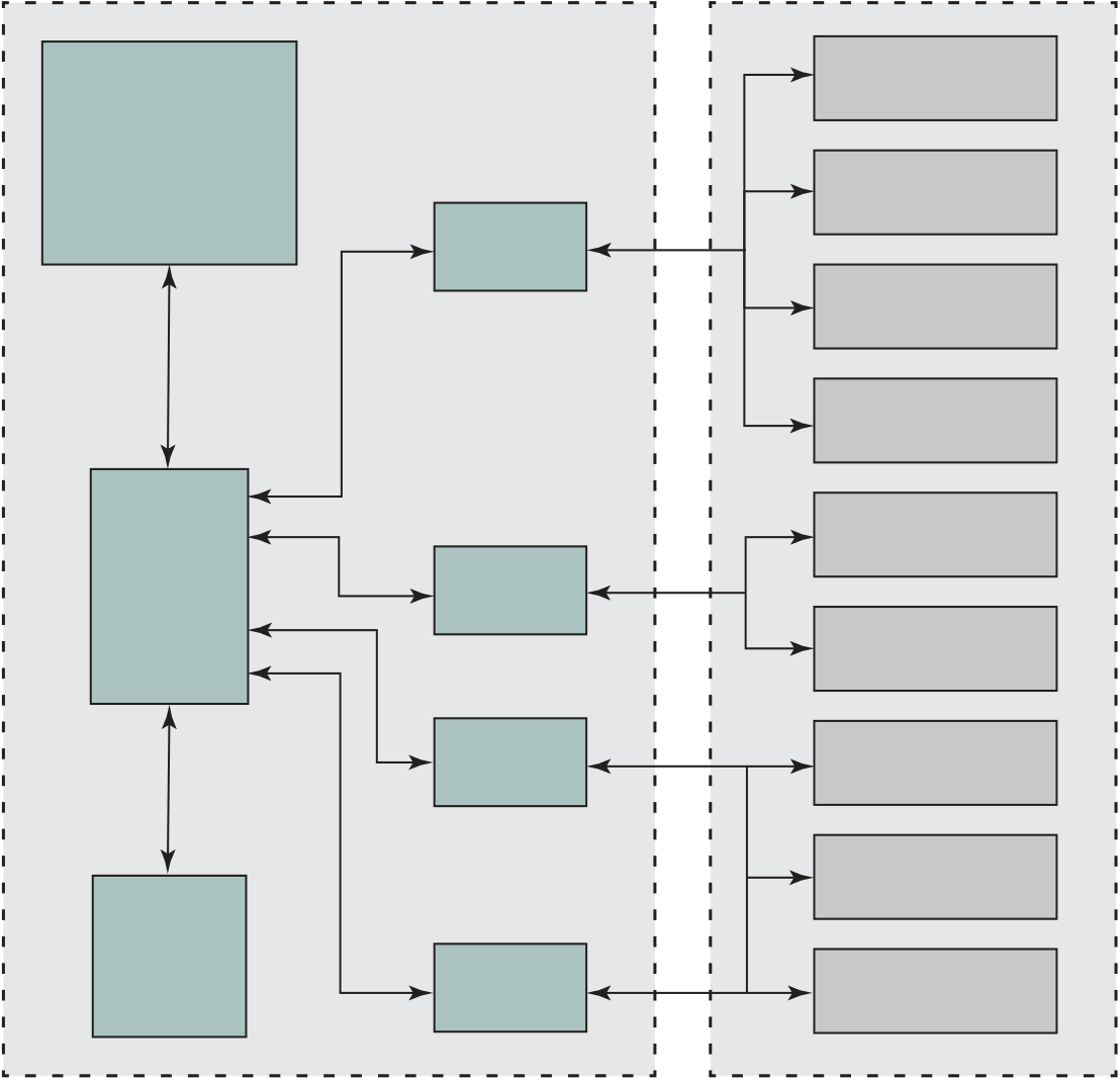
At a top level, a computer consists of CPU (central processing unit), memory, and I/O components, with one or more modules of each type. These components are interconnected in some fashion to achieve the basic function of the computer, which is to execute programs. Thus, at a top level, we can characterize a computer system by describing (1) the external behavior of each component, that is, the data and control signals that it exchanges with other components, and (2) the intercon-nection structure and the controls required to manage the use of the interconnec-tion structure.
■ Data and instructions are stored in a single read–write memory.
■ The contents of this memory are addressable by location, without regard to the type of data contained there.
Now consider this alternative. Suppose we construct a general-purpose con-figuration of arithmetic and logic functions. This set of hardware will perform vari-ous functions on data depending on control signals applied to the hardware. In the original case of customized hardware, the system accepts data and produces results (Figure 3.1a). With general-purpose hardware, the system accepts data and control signals and produces results. Thus, instead of rewiring the hardware for each new program, the programmer merely needs to supply a new set of control signals.
How shall control signals be supplied? The answer is simple but subtle. The entire program is actually a sequence of steps. At each step, some arithmetic or logical operation is performed on some data. For each step, a new set of control sig-nals is needed. Let us provide a unique code for each possible set of control signals,
| Data | Sequence of | Results |
|---|---|---|
| arithmetic | ||
| and logic | ||
| functions |
| Data | General-purpose | Results |
|---|---|---|
| arithmetic | ||
| and logic | ||
| functions |
(b) Programming in software
Figure 3.1 Hardware and Software Approaches
One more component is needed. An input device will bring instructions and data in sequentially. But a program is not invariably executed sequentially; it may jump around (e.g., the IAS jump instruction). Similarly, operations on data may require access to more than just one element at a time in a predetermined sequence. Thus, there must be a place to temporarily store both instructions and data. That module is called memory, or main memory, to distinguish it from external storage or peripheral devices. Von Neumann pointed out that the same memory could be used to store both instructions and data.
Figure 3.2 illustrates these top-level components and suggests the interac-tions among them. The CPU exchanges data with memory. For this purpose, it typ-ically makes use of two internal (to the CPU) registers: a memory address register (MAR), which specifies the address in memory for the next read or write, and a memory buffer register (MBR), which contains the data to be written into memory or receives the data read from memory. Similarly, an I/O address register (I/OAR) specifies a particular I/O device. An I/O buffer register (I/OBR) is used for the exchange of data between an I/O module and the CPU.
84 Chapter 3 / a top-LeveL view of Computer funCtion and interConneCtion
| IR | Instruction |
|---|
I/O AR
| PC | = |
|---|
At the beginning of each instruction cycle, the processor fetches an instruction from memory. In a typical processor, a register called the program counter (PC) holds the address of the instruction to be fetched next. Unless told otherwise, the processor
| Fetch cycle | HALT | ||
|---|---|---|---|
| Fetch next | Execute | ||
| instruction | instruction |
always increments the PC after each instruction fetch so that it will fetch the next instruction in sequence (i.e., the instruction located at the next higher memory address). So, for example, consider a computer in which each instruction occupies one 16-bit word of memory. Assume that the program counter is set to memory loca-tion 300, where the location address refers to a 16-bit word. The processor will next fetch the instruction at location 300. On succeeding instruction cycles, it will fetch instructions from locations 301, 302, 303, and so on. This sequence may be altered, as explained presently.
The fetched instruction is loaded into a register in the processor known as the instruction register (IR). The instruction contains bits that specify the action the processor is to take. The processor interprets the instruction and performs the required action. In general, these actions fall into four categories:
An instruction’s execution may involve a combination of these actions.
Consider a simple example using a hypothetical machine that includes the characteristics listed in Figure 3.4. The processor contains a single data register, called an accumulator (AC). Both instructions and data are 16 bits long. Thus, it is convenient to organize memory using 16-bit words. The instruction format provides 4 bits for the opcode, so that there can be as many as 24= 16 different opcodes, and up to 212= 4096 (4K) words of memory can be directly addressed.
| Opcode | Address |
|---|
(a) Instruction format
| Magnitude |
|---|
0001 = Load AC from memory
0010 = Store AC to memory
0101 = Add to AC from memory(d) Partial list of opcodes Figure 3.4 Characteristics of a Hypothetical Machine
1. The PC contains 300, the address of the first instruction. This instruction (the value 1940 in hexadecimal) is loaded into the instruction register IR, and the PC is incremented. Note that this process involves the use of a memory address register and a memory buffer register. For simplicity, these intermedi-ate registers are ignored.
2. The first 4 bits (first hexadecimal digit) in the IR indicate that the AC is to be loaded. The remaining 12 bits (three hexadecimal digits) specify the address (940) from which data are to be loaded.
In this example, three instruction cycles, each consisting of a fetch cycle and an execute cycle, are needed to add the contents of location 940 to the contents of 941. With a more complex set of instructions, fewer cycles would be needed. Some older processors, for example, included instructions that contain more than one memory address. Thus, the execution cycle for a particular instruction on such processors could involve more than one reference to memory. Also, instead of memory refer-ences, an instruction may specify an I/O operation.
For example, the PDP-11 processor includes an instruction, expressed symboli-cally as ADD B,A, that stores the sum of the contents of memory locations B and A into memory location A. A single instruction cycle with the following steps occurs:
■ Write the result from the processor to memory location A.
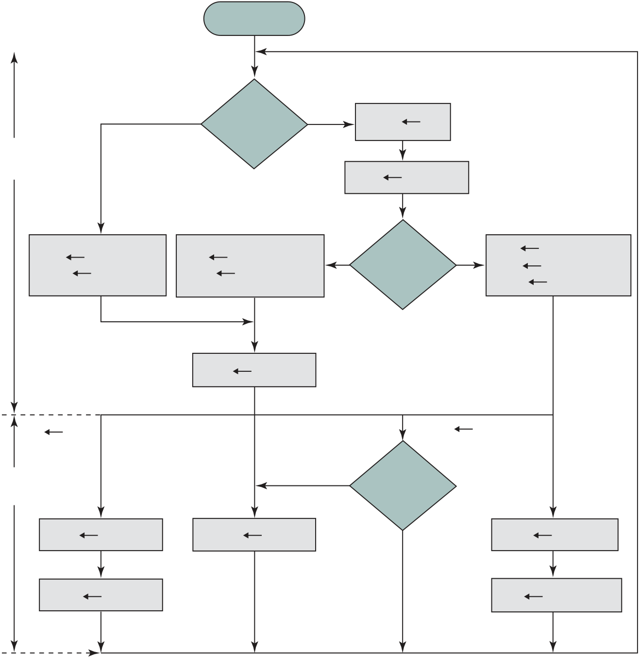
Thus, the execution cycle for a particular instruction may involve more than one reference to memory. Also, instead of memory references, an instruction may specify an I/O operation. With these additional considerations in mind, Figure 3.6 provides a more detailed look at the basic instruction cycle of Figure 3.3. The figure is in the form of a state diagram. For any given instruction cycle, some states may be null and others may be visited more than once. The states can be described as follows:
|
|
|||
|---|---|---|---|---|
| store | ||||
| Instruction | Instruction | Multiple | Multiple | |
| operands | results | |||
|
||||
| address | operation |
|
||
| calculation | decoding | |||
| Instruction complete, | Return for string | |||
| fetch next instruction | or vector data | |||
■ Instruction operation decoding (iod): Analyze instruction to determine type of operation to be performed and operand(s) to be used.
■ Operand address calculation (oac): If the operation involves reference to an operand in memory or available via I/O, then determine the address of the operand.
Also note that the diagram allows for multiple operands and multiple results, because some instructions on some machines require this. For example, the PDP-11 instruction ADD A,B results in the following sequence of states: iac, if, iod, oac, of, oac, of, do, oac, os.
Finally, on some machines, a single instruction can specify an operation to be per-formed on a vector (one-dimensional array) of numbers or a string (one-dimensional
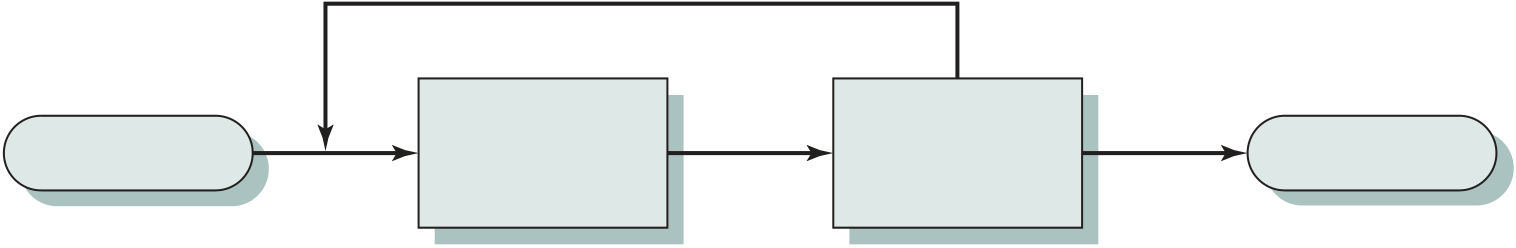
Interrupts are provided primarily as a way to improve processing efficiency. For example, most external devices are much slower than the processor. Suppose that the processor is transferring data to a printer using the instruction cycle scheme of Figure 3.3. After each write operation, the processor must pause and remain idle until the printer catches up. The length of this pause may be on the order of many hundreds or even thousands of instruction cycles that do not involve memory. Clearly, this is a very wasteful use of the processor.
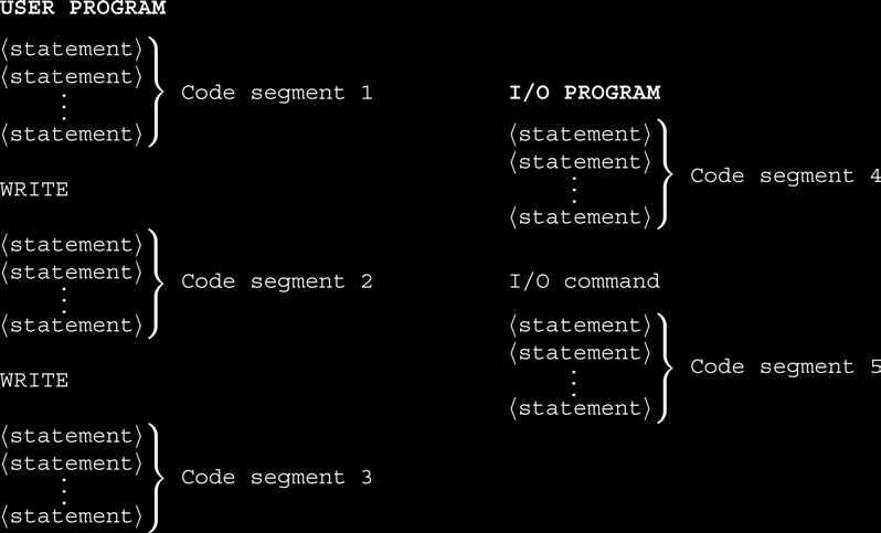
Figure 3.7a illustrates this state of affairs. The user program performs a ser-ies of WRITE calls interleaved with processing. Code segments 1, 2, and 3 refer to sequences of instructions that do not involve I/O. The WRITE calls are to an I/O program that is a system utility and that will perform the actual I/O operation. The I/O program consists of three sections:
|
|
||||
|---|---|---|---|---|---|
| 1 | 4 | 4 |
|
4 | |
|
|||||
| WRITE |
5
2a
3a
3 3 3b
| WRITE | |||
|---|---|---|---|
| (b) Interrupts; short I/O wait |
= interrupt occurs during course of execution of user program
Figure 3.7 Program Flow of Control without and with Interrupts
3.2 / Computer funCtion 91
•
•
•
M
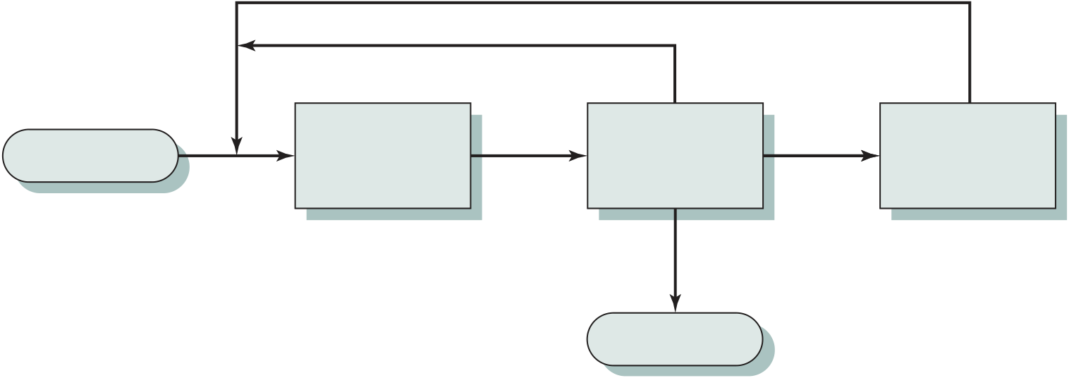
| Fetch cycle | Execute cycle | Interrupt cycle |
|---|
Interrupts
disabled
3.2 / Computer funCtion 93
(current contents of the program counter) and any other data relevant to the processor’s current activity.
Time
| 1 |
|
1 | ||
|---|---|---|---|---|
| 4 | 4 | |||
| 5 | 2a | |||
| processor executing | ||||
| 5 |
2
4
(b) With interrupts
3
shaded gray. Figure 3.10a shows the case in which interrupts are not used. The pro-cessor must wait while an I/O operation is performed.
Figures 3.7b and 3.10b assume that the time required for the I/O operation is rela-tively short: less than the time to complete the execution of instructions between write operations in the user program. In this case, the segment of code labeled code segment 2 is interrupted. A portion of the code (2a) executes (while the I/O operation is performed) and then the interrupt occurs (upon the completion of the I/O operation). After the inter-rupt is serviced, execution resumes with the remainder of code segment 2 (2b).
| 1 | 1 | |||
|---|---|---|---|---|
| 4 | 4 | |||
| 2 | ||||
|
|
|||
| processor executing; |
3 I/O operation
concurrent with I/O operation; processor executing; processor waits then processor waits
5 |
|---|
Figure 3.11 Program Timing: Long I/O Wait
3.2 / Computer funCtion 95
The drawback to the preceding approach is that it does not take into account relative priority or time-critical needs. For example, when input arrives from the communications line, it may need to be absorbed rapidly to make room for more input. If the first batch of input has not been processed before the second batch arrives, data may be lost.
A second approach is to define priorities for interrupts and to allow an interrupt of higher priority to cause a lower-priority interrupt handler to be itself interrupted (Figure 3.13b). As an example of this second approach, consider a system with three I/O devices: a printer, a disk, and a communications line, with increasing priori-ties of 2, 4, and 5, respectively. Figure 3.14 illustrates a possible sequence. A user program begins at t = 0. At t = 10, a printer interrupt occurs; user information is placed on the system stack and execution continues at the printer interrupt service routine (ISR). While this routine is still executing, at t = 15, a communications inter-rupt occurs. Because the communications line has higher priority than the printer, the interrupt is honored. The printer ISR is interrupted, its state is pushed onto the stack, and execution continues at the communications ISR. While this routine is exe-cuting, a disk interrupt occurs (t = 20). Because this interrupt is of lower priority, it is simply held, and the communications ISR runs to completion.
Figure 3.12 Instruction Cycle State Diagram, with Interrupts
handler Y
(a) Sequential interrupt processing
(b) Nested interrupt processing
Figure 3.13 Transfer of Control with Multiple Interrupts
| Printer |
|
|
|---|---|---|
| interrupt | interrupt | |
| service routine |
|
I/O Function
Thus far, we have discussed the operation of the computer as controlled by the pro-cessor, and we have looked primarily at the interaction of processor and memory. The discussion has only alluded to the role of the I/O component. This role is dis-cussed in detail in Chapter 7, but a brief summary is in order here.
3.3 interConneCtion struCtures
A computer consists of a set of components or modules of three basic types (pro-cessor, memory, I/O) that communicate with each other. In effect, a computer is a network of basic modules. Thus, there must be paths for connecting the modules.
Write
N words
| Data | • | |
|---|---|---|
| N� 1 | ||
| Read | I/O module | |
| Write | M ports | |
| Address | ||
|
||
|
||
| CPU | ||
| Instructions | ||
|
||
| Data |
|
|
100 Chapter 3 / a top-LeveL view of Computer funCtion and interConneCtion
is indicated by read and write control signals. The location for the operation is specified by an address.
■ Processor to memory: The processor writes a unit of data to memory.
■ I/O to processor: The processor reads data from an I/O device via an I/O module.
The bus was the dominant means of computer system component interconnection for decades. For general-purpose computers, it has gradually given way to various point-to-point interconnection structures, which now dominate computer system design. However, bus structures are still commonly used for embedded systems, par-ticularly microcontrollers. In this section, we give a brief overview of bus structure. Appendix C provides more detail.
A bus is a communication pathway connecting two or more devices. A key characteristic of a bus is that it is a shared transmission medium. Multiple devices connect to the bus, and a signal transmitted by any one device is available for recep-tion by all other devices attached to the bus. If two devices transmit during the same time period, their signals will overlap and become garbled. Thus, only one device at a time can successfully transmit.
A system bus consists, typically, of from about fifty to hundreds of separate lines. Each line is assigned a particular meaning or function. Although there are many different bus designs, on any bus the lines can be classified into three func-tional groups (Figure 3.16): data, address, and control lines. In addition, there may be power distribution lines that supply power to the attached modules.
The data lines provide a path for moving data among system modules. These lines, collectively, are called the data bus. The data bus may consist of 32, 64, 128, or even more separate lines, the number of lines being referred to as the width of the data bus. Because each line can carry only one bit at a time, the number of lines determines how many bits can be transferred at a time. The width of the data bus is a key factor in determining overall system performance. For example, if the data bus is 32 bits wide and each instruction is 64 bits long, then the processor must access the memory module twice during each instruction cycle.
Control lines
there must be a means of controlling their use. Control signals transmit both com-mand and timing information among system modules. Timing signals indicate the validity of data and address information. Command signals specify operations to be performed. Typical control lines include:
■ Memory write: causes data on the bus to be written into the addressed location.
■ Bus request: indicates that a module needs to gain control of the bus.
■ Bus grant: indicates that a requesting module has been granted control of the bus.
The operation of the bus is as follows. If one module wishes to send data to another, it must do two things: (1) obtain the use of the bus, and (2) transfer data via the bus. If one module wishes to request data from another module, it must (1) obtain the use of the bus, and (2) transfer a request to the other module over the appropriate control and address lines. It must then wait for that second module to send the data.
3.5 point-to-point interConneCt
3.5 / point-to-point interConneCt 103
The following are significant characteristics of QPI and other point-to-point interconnect schemes:
In addition, QPI is used to connect to an I/O module, called an I/O hub (IOH). The IOH acts as a switch directing traffic to and from I/O devices. Typically in newer
| I/O device | I/O Hub |
|
I/O device |
|---|---|---|---|
| DRAM | DRAM | ||
| B | |||
| DRAM | DRAM | ||
|
D | ||
|
I/O Hub | ||
| PCI Express | |||
| QPI |
104 Chapter 3 / a top-LeveL view of Computer funCtion and interConneCtion
■ Link: Responsible for reliable transmission and flow control. The Link layer’s unit of transfer is an 80-bit Flit (flow control unit).
■ Routing: Provides the framework for directing packets through the fabric.
3.5 / point-to-point interConneCt 105
| Fwd Clk | Reception Lanes | Rcv Clk | |
|---|---|---|---|
|
Transmission Lanes |
|
The form of transmission on each lane is known as differential signaling, or balanced transmission. With balanced transmission, signals are transmitted as a cur-rent that travels down one conductor and returns on the other. The binary value depends on the voltage difference. Typically, one line has a positive voltage value and the other line has zero voltage, and one line is associated with binary 1 and one line is associated with binary 0. Specifically, the technique used by QPI is known as low-voltage differential signaling (LVDS). In a typical implementation, the trans-mitter injects a small current into one wire or the other, depending on the logic level to be sent. The current passes through a resistor at the receiving end, and then returns in the opposite direction along the other wire. The receiver senses the polar-ity of the voltage across the resistor to determine the logic level.
Another function performed by the physical layer is that it manages the trans-lation between 80-bit flits and 20-bit phits using a technique known as multilane distribution. The flits can be considered as a bit stream that is distributed across the data lanes in a round-robin fashion (first bit to first lane, second bit to second lane, etc.), as illustrated in Figure 3.20. This approach enables QPI to achieve very high data rates by implementing the physical link between two ports as multiple parallel channels.
Figure 3.20 QPI Multilane Distribution
an 8-bit error control code called a cyclic redundancy check (CRC). We discuss error control codes in Chapter 5.
2. When a flit is received, B calculates a CRC value for the 72-bit payload and compares this value with the value of the incoming CRC value in the flit. If the two CRC values do not match, an error has been detected.
3. When B detects an error, it sends a request to A to retransmit the flit that is in error. However, because A may have had sufficient credit to send a stream of flits, so that additional flits have been transmitted after the flit in error and
QPI Protocol Layer
In this layer, the packet is defined as the unit of transfer. The packet contents definition is standardized with some flexibility allowed to meet differing market segment require-ments. One key function performed at this level is a cache coherency protocol, which deals with making sure that main memory values held in multiple caches are consistent. A typical data packet payload is a block of data being sent to or from a cache.
A key requirement for PCIe is high capacity to support the needs of higher data rate I/O devices, such as Gigabit Ethernet. Another requirement deals with the need to support time-dependent data streams. Applications such as video-on- demand and audio redistribution are putting real-time constraints on servers too. Many communications applications and embedded PC control systems also pro-cess data in real-time. Today’s platforms must also deal with multiple concurrent
■ Switch: The switch manages multiple PCIe streams.
■ PCIe endpoint: An I/O device or controller that implements PCIe, such as a Gigabit ethernet switch, a graphics or video controller, disk interface, or a communications controller.
| Gigabit | PCIe | Core | Memory | |
|---|---|---|---|---|
| ethernet |
| Legacy |
|
Switch | PCIe | PCIe |
|
|---|---|---|---|---|---|
| PCIe | |||||
| PCIe | |||||
| endpoint | endpoint |
3.6 / pCi express 109
■ Data link: Is responsible for reliable transmission and flow control. Data pack-ets generated and consumed by the DLL are called Data Link Layer Packets (DLLPs).
■ Transaction: Generates and consumes data packets used to implement load/ store data transfer mechanisms and also manages the flow control of those packets between the two components on a link. Data packets generated and consumed by the TL are called Transaction Layer Packets (TLPs).
Transaction layer
| Data link | packets (DLLPs) | |
|---|---|---|
| Physical |
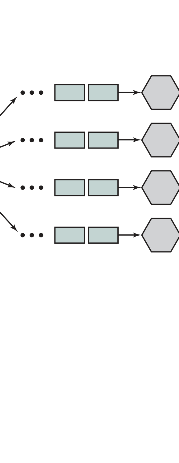
byte stream
| B7 | B6 | B5 | B4 | B3 | B2 | B1 | B5 | B1 | 128b/ | PCIe | |
|---|---|---|---|---|---|---|---|---|---|---|---|
| 130b | lane 1 | ||||||||||
| B6 | B2 | PCIe | |||||||||
| 128b/ | |||||||||||
| 130b | lane 2 | ||||||||||
| B7 | B3 | PCIe | |||||||||
| 128b/ | |||||||||||
| 130b | lane 3 |
To understand the rationale for the 128b/130b encoding, note that unlike QPI, PCIe does not use its clock line to synchronize the bit stream. That is, the clock line is not used to determine the start and end point of each incoming bit; it is used for other signaling purposes only. However, it is necessary for the receiver to be syn-chronized with the transmitter, so that the receiver knows when each bit begins and ends. If there is any drift between the clocks used for bit transmission and reception of the transmitter and receiver, errors may occur. To compensate for the possibil-ity of drift, PCIe relies on the receiver synchronizing with the transmitter based on the transmitted signal. As with QPI, PCIe uses differential signaling over a pair of wires. Synchronization can be achieved by the receiver looking for transitions in the data and synchronizing its clock to the transition. However, consider that with a long string of 1s or 0s using differential signaling, the output is a constant voltage over a long period of time. Under these circumstances, any drift between the clocks of transmitter and receiver will result in loss of synchronization between the two.
A common approach, and the one used in PCIe 3.0, to overcoming the prob-lem of a long string of bits of one value is scrambling. Scrambling, which does not increase the number of bits to be transmitted, is a mapping technique that tends to make the data appear more random. The scrambling tends to spread out the num-ber of transitions so that they appear at the receiver more uniformly spaced, which is good for synchronization. Also, other transmission properties, such as spectral properties, are enhanced if the data are more nearly of a random nature rather than constant or repetitive. For more discussion of scrambling, see Appendix E.
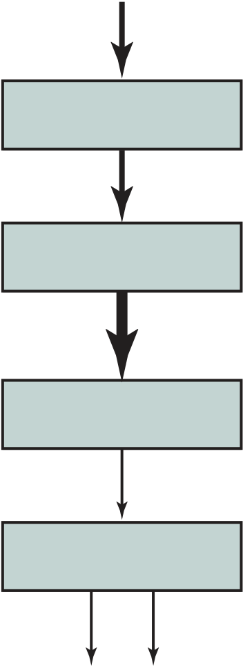
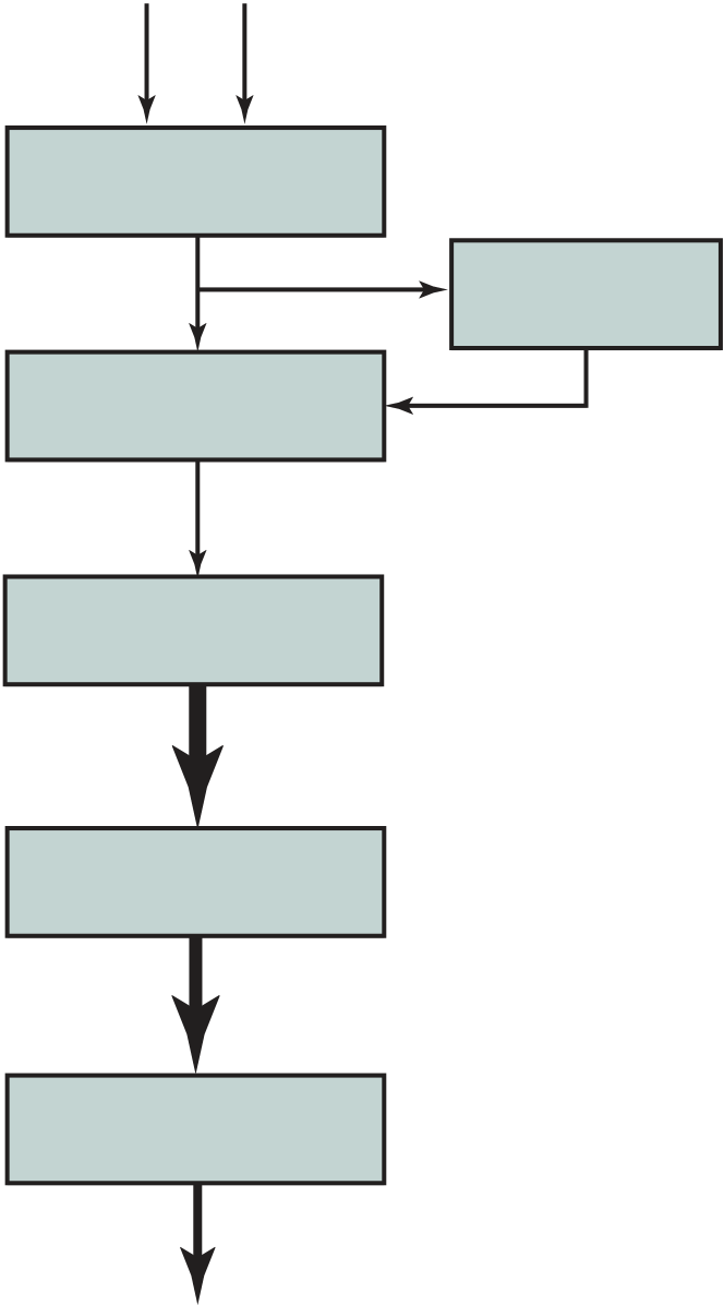
112 Chapter 3 / a top-LeveL view of Computer funCtion and interConneCtion
128b
| D+ |
|
Descrambler |
|---|---|---|
| (a) Transmitter | ||
The transaction layer (TL) receives read and write requests from the software above the TL and creates request packets for transmission to a destination via the link layer. Most transactions use a split transaction technique, which works in the follow-ing fashion. A request packet is sent out by a source PCIe device, which then waits for a response, called a completion packet. The completion following a request is initiated by the completer only when it has the data and/or status ready for delivery. Each packet has a unique identifier that enables completion packets to be directed to the correct originator. With the split transaction technique, the completion is sep-arated in time from the request, in contrast to a typical bus operation in which both sides of a transaction must be available to seize and use the bus. Between the request and the completion, other PCIe traffic may use the link.
TL messages and some write transactions are posted transactions, meaning that no response is expected.
■ Memory: The memory space includes system main memory. It also includes PCIe I/O devices. Certain ranges of memory addresses map into I/O devices.
■ I/O: This address space is used for legacy PCI devices, with reserved memory address ranges used to address legacy I/O devices.
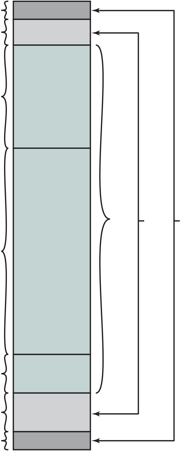
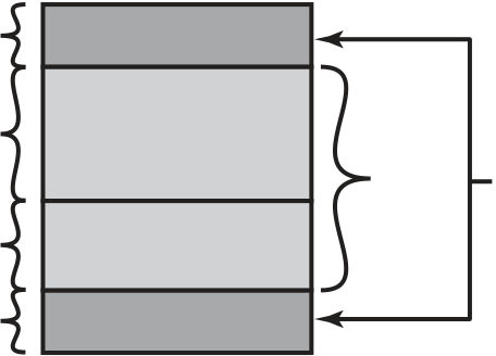
tlppacketassembly PCIe transactions are conveyed using transaction layer packets, which are illustrated in Figure 3.25a. A TLP originates in the transaction layer of the sending device and terminates at the transaction layer of the receiving device.
Number
| STP framing | Created by Transaction Layer | Appended by Data Link Layer | 1 | Start | Created | by DLL | Appended by PL | |
|---|---|---|---|---|---|---|---|---|
| 2 | Sequence number | 4 | DLLP | |||||
| 12 or 16 | Header | 2 | CRC | |||||
| 1 | End | |||||||
| 0 to 4096 | Data | |||||||
| 0 or 4 | ECRC |
Figure 3.25 PCIe Protocol Data Unit Format
3.6 / pCi express 115
PCIe Data Link Layer
The purpose of the PCIe data link layer is to ensure reliable delivery of packets across the PCIe link. The DLL participates in the formation of TLPs and also trans-mits DLLPs.
2. If an error is detected, the DLL schedules an NAK DLL packet to return back to the remote transmitter. The TLP is eliminated.
When the DLL transmits a TLP, it retains a copy of the TLP. If it receives an NAK for the TLP with this sequence number, it retransmits the TLP. When it receives an ACK, it discards the buffered TLP.
|
|---|
2. Add contents of memory location 940.
3. Store AC to device 6.
3.4 3.5 |
c. How many bits are needed for the program counter and the instruction register?
|
|---|
118 Chapter 3 / a top-LeveL view of Computer funCtion and interConneCtion
| Bus |
|
BPRO | BPRN | BPRO | BPRN | BPRO | Bus |
|---|---|---|---|---|---|---|---|
| terminator | terminator | ||||||
| Master 2 | |||||||
| Master 3 | |||||||
cycle, any agent can request control of the bus by lowering its BPRO line. This lowers the BPRN line of the next agent in the chain, which is in turn required to lower its BPRO line. Thus, the signal is propagated the length of the chain. At the end of this chain reaction, there should be only one agent whose BPRN is asserted and whose BPRO is not. This agent has priority. If, at the beginning of a bus cycle, the bus is not busy (BUSY inactive), the agent that has priority may seize control of the bus by asserting the BUSY line.
It takes a certain amount of time for the BPR signal to propagate from the highest-priority agent to the lowest. Must this time be less than the clock cycle? Explain.
3.15 3.16 |
|
|---|
4.1 Computer Memory System Overview Characteristics of Memory Systems The Memory Hierarchy
4.2 Cache Memory Principles
120
4.1 / Computer memory SyStem overview 121
4.1 COMPUTER MEMORY SYSTEM OVERVIEW
Characteristics of Memory Systems
Table 4.1 Key Characteristics of Computer Memory Systems
|
|---|
Another distinction among memory types is the method of accessing units of data. These include the following:
■ Sequential access: Memory is organized into units of data, called records. Access must be made in a specific linear sequence. Stored addressing infor-mation is used to separate records and assist in the retrieval process. A shared read– write mechanism is used, and this must be moved from its current loca-tion to the desired location, passing and rejecting each intermediate record. Thus, the time to access an arbitrary record is highly variable. Tape units, dis-cussed in Chapter 6, are sequential access.
■ Associative: This is a random access type of memory that enables one to make a comparison of desired bit locations within a word for a specified match, and to do this for all words simultaneously. Thus, a word is retrieved based on a portion of its contents rather than its address. As with ordinary random- access memory, each location has its own addressing mechanism, and retrieval time is constant independent of location or prior access patterns. Cache memories may employ associative access.
From a user’s point of view, the two most important characteristics of memory are capacity and performance. Three performance parameters are used:
Tn = Average time to read or writenbits
TA = Average access time
Several physical characteristics of data storage are important. In a volatile memory, information decays naturally or is lost when electrical power is switched off. In a nonvolatile memory, information once recorded remains without deterio-ration until deliberately changed; no electrical power is needed to retain informa-tion. Magnetic- surface memories are nonvolatile. Semiconductor memory (memory on integrated circuits) may be either volatile or nonvolatile. Nonerasable memory cannot be altered, except by destroying the storage unit. Semiconductor memory of this type is known as read- only memory (ROM). Of necessity, a practical nonerasa-ble memory must also be nonvolatile.
For random- access memory, the organization is a key design issue. In this con-text, organization refers to the physical arrangement of bits to form words. The obvious arrangement is not always used, as is explained in Chapter 5.
■ Faster access time, greater cost per bit;
■ Greater capacity, smaller cost per bit;
b. Increasing capacity;
c. Increasing access time;
Figure 4.1 The Memory Hierarchy
is item (d): decreasing frequency of access. We examine this concept in greater detail when we discuss the cache, later in this chapter, and virtual memory in Chapter 8. A brief explanation is provided at this point.
memory contain all program instructions and data. The current clusters can be tem-porarily placed in level 1. From time to time, one of the clusters in level 1 will have to be swapped back to level 2 to make room for a new cluster coming in to level 1. On average, however, most references will be to instructions and data contained in level 1.
This principle can be applied across more than two levels of memory, as sug-gested by the hierarchy shown in Figure 4.1. The fastest, smallest, and most expen-sive type of memory consists of the registers internal to the processor. Typically, a processor will contain a few dozen such registers, although some machines contain hundreds of registers. Main memory is the principal internal memory system of the computer. Each location in main memory has a unique address. Main memory is usu-ally extended with a higher- speed, smaller cache. The cache is not usually visible to the programmer or, indeed, to the processor. It is a device for staging the movement of data between main memory and processor registers to improve performance.
Appendix 4A examines the performance implications of multilevel memory structures.
2 Disk cache is generally a purely software technique and is not examined in this book. See [STAL15] for a discussion.
Figure 4.3b depicts the use of multiple levels of cache. The L2 cache is slower and typically larger than the L1 cache, and the L3 cache is slower and typically larger than the L2 cache.
Figure 4.4 depicts the structure of a cache/ main- memory system. Main mem-ory consists of up to 2n addressable words, with each word having a unique n- bit address. For mapping purposes, this memory is considered to consist of a number of fixed- length blocks of K words each. That is, there are M = 2n/K blocks in main memory. The cache consists of m blocks, called lines.3 Each line contains K words,
| CPU | Level 1 | Level 2 | Level 3 | Main |
|---|---|---|---|---|
| (L1) cache | (L2) cache | (L3) cache |
|
(b) Three-level cache organization
|
Memory |
|
||||||
|---|---|---|---|---|---|---|---|---|
| address | ||||||||
| 0 | ||||||||
| 1 | ||||||||
| 2 | ||||||||
| 3 | (K words) | |||||||
| Block length | • | |||||||
| (K words) | ||||||||
| (a) Cache | • | |||||||
| • | ||||||||
Figure 4.4 Cache/Main Memory Structure
plus a tag of a few bits. Each line also includes control bits (not shown), such as a bit to indicate whether the line has been modified since being loaded into the cache. The length of a line, not including tag and control bits, is the line size. The line size may be as small as 32 bits, with each “word” being a single byte; in this case the line size is 4 bytes. The number of lines is considerably less than the number of main memory blocks (m V M). At any time, some subset of the blocks of mem-ory resides in lines in the cache. If a word in a block of memory is read, that block is transferred to one of the lines of the cache. Because there are more blocks than lines, an individual line cannot be uniquely and permanently dedicated to a par-ticular block. Thus, each line includes a tag that identifies which particular block is currently being stored. The tag is usually a portion of the main memory address, as described later in this section.
Receive address
RA from CPU
|
Access main | |
|---|---|---|
| containing RA | memory for block | |
| containing RA |
which main memory is reached. When a cache hit occurs, the data and address buff-ers are disabled and communication is only between processor and cache, with no system bus traffic. When a cache miss occurs, the desired address is loaded onto the system bus and the data are returned through the data buffer to both the cache and the processor. In other organizations, the cache is physically interposed between the processor and the main memory for all data, address, and control lines. In this latter case, for a cache miss, the desired word is first read into the cache and then transferred from cache to processor.
A discussion of the performance parameters related to cache use is contained in Appendix 4A.
| Processor | Control | Cache | Control | System bus |
|---|
Data
buffer
Data
Almost all nonembedded processors, and many embedded processors, support vir-tual memory, a concept discussed in Chapter 8. In essence, virtual memory is a facil-ity that allows programs to address memory from a logical point of view, without regard to the amount of main memory physically available. When virtual memory is used, the address fields of machine instructions contain virtual addresses. For reads
4For a general discussion of HPC, see [DOWD98].
to and writes from main memory, a hardware memory management unit (MMU) translates each virtual address into a physical address in main memory.
When virtual addresses are used, the system designer may choose to place the cache between the processor and the MMU or between the MMU and main mem-ory (Figure 4.7). A logical cache, also known as a virtual cache, stores data using
| Logical address | MMU | Physical address | Main | |
|---|---|---|---|---|
| Cache | memory |
Data
(b) Physical cache
The subject of logical versus physical cache is a complex one, and beyond the scope of this book. For a more in- depth discussion, see [CEKL97] and [JACO08].
Cache Size
Table 4.3 Cache Sizes of Some Processors
i = cache line number
j = main memory block number
| B0 | b |
m lines |
||
|---|---|---|---|---|
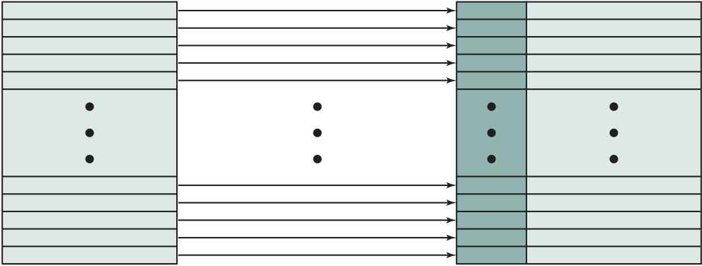 |
||||
| Bm–1 | Lm–1 | |||
| First m blocks of | Cache memory | |||
main memory
b = length of block in bits
t = length of tag in bits(a) Direct mapping
Figure 4.8 Mapping from Main Memory to Cache: Direct and Associative
of main memory map into the cache in the same fashion; that is, block Bm of main memory maps into line L0 of cache, block Bm+1 maps into line L1, and so on.
|
|
|---|
| 1 if match | (Hit in cache) |
|
Li | s | W4j | Bj | |
|---|---|---|---|---|---|---|---|
| w |
|
||||||
| W(4j+3) |
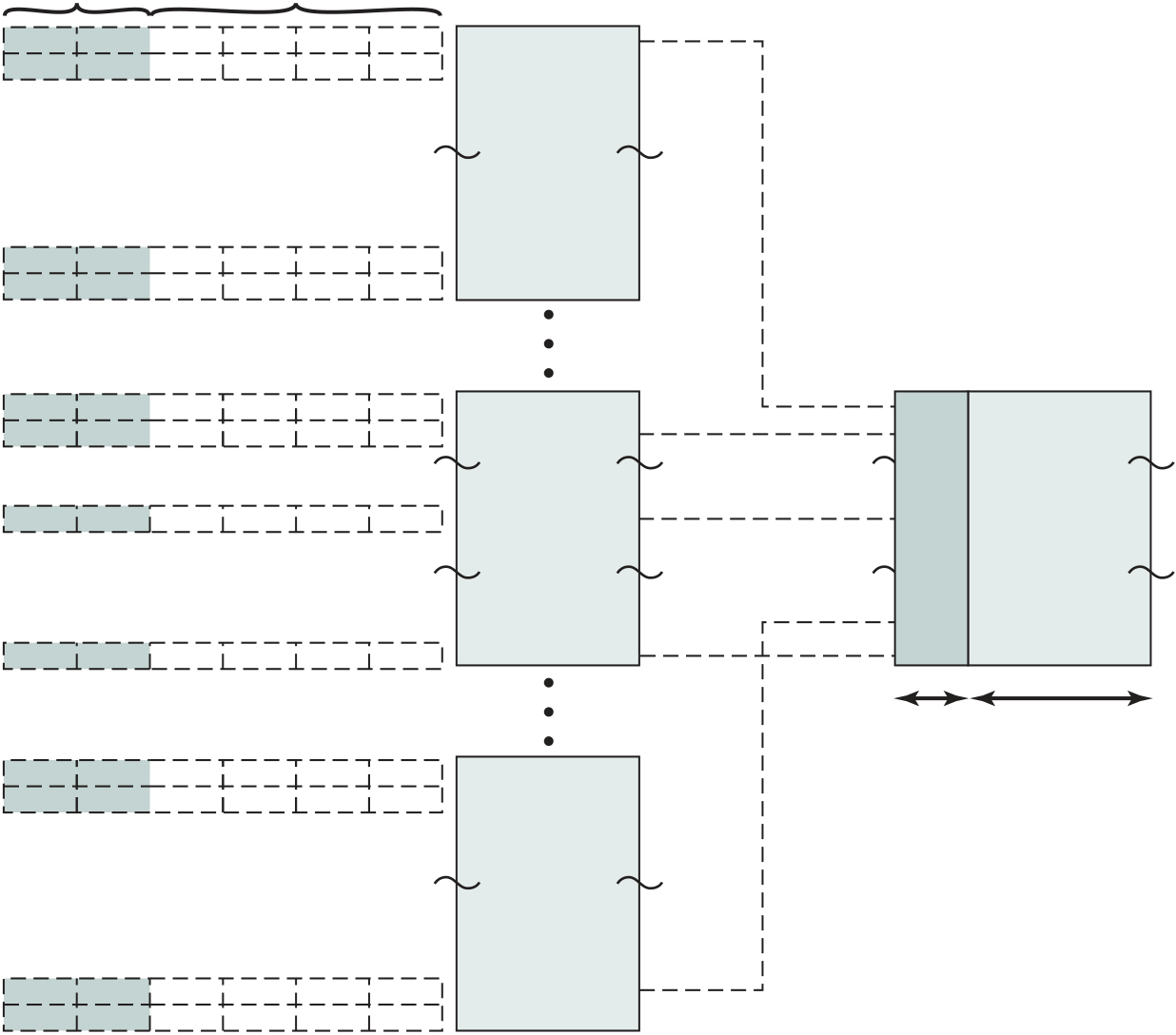
4.3 / elementS of CACHe DeSign 137 Main memory address (binary)
16 16 |
|||||||||
|---|---|---|---|---|---|---|---|---|---|
| Tag | Line + Word |
|
|||||||
|
|||||||||
| Tag | Data | Line | |||||||
| number | |||||||||
|
13579246 11235813 | 0000 0001 | |||||||
|
16 | FEDCBA98 FEDCBA98 | 0CE7 | ||||||
| FF | 11223344 | 3FFE | |||||||
| 16 | 12345678 | 3FFF | |||||||
| 8 bits | |||||||||
|
16K line cache | ||||||||
|
|||||||||
|
|||||||||
| 16-Mb main memory | |||||||||
| Tag | Line |
|
|||||||
| Main memory address = | |||||||||
The direct mapping technique is simple and inexpensive to implement. Its main disadvantage is that there is a fixed cache location for any given block. Thus, if a program happens to reference words repeatedly from two different blocks that map into the same line, then the blocks will be continually swapped in the cache,
| and the hit ratio will be low (a phenomenon known as thrashing). |
|---|

| w | Lj | s | Bj | ||
|---|---|---|---|---|---|
|
Lm–1 | w | |||
|
|||||
| 1 if match | |||||
| s | |||||
| 0 if no match |
Note that no field in the address corresponds to the line number, so that the number of lines in the cache is not determined by the address format. To summarize,
■ Address length = (s + w) bits
■ Number of addressable units = 2s+w words or bytes■ Block size = line size = 2w words or bytes
■ Number of blocks in main memory =2s+w 2w = 2s
 |
|---|
set- associativemapping Set- associative mapping is a compromise that exhibits the strengths of both the direct and associative approaches while reducing their disadvantages.
In this case, the cache consists of number sets, each of which consists of a num-ber of lines. The relationships are
j = main memory block number
m = number of lines in the cache
4.3 / elementS of CACHe DeSign 141
Cache memory–set v–1
(a) v associative–mapped caches
| B0 | L0 | |||
|---|---|---|---|---|
| Bv–1 | ||||
| One | ||||
| set | ||||
|
||||
|
For set- associative mapping, the cache control logic interprets a memory address as three fields: Tag, Set, and Word. The d set bits specify one of v = 2d sets. The s bits of the Tag and Set fields specify one of the 2s blocks of main memory. Figure 4.14 illustrates the cache control logic. With fully associative mapping, the tag in a memory address is quite large and must be compared to the tag of every line in the cache. With k- way set- associative mapping, the tag in a memory address is much smaller and is only compared to the k tags within a single set. To summarize,
■ Address length = (s + w) bits
■ Number of addressable units = 2s+w words or bytes
|
Fk–1 | Set 1 | s + w | Bj | ||
|---|---|---|---|---|---|---|
| Fk | ||||||
| Fk+i | ||||||
| 1 if match | F2k–1 |
0 if no match
■ Block size = line size = 2w words or bytes
■ Number of blocks in main memory =2s+w 2w = 2s
| Hit ratio | 1.0 | |||||||||||
|---|---|---|---|---|---|---|---|---|---|---|---|---|
| 0.9 | ||||||||||||
| 0.8 | ||||||||||||
| 0.7 | ||||||||||||
| 0.6 | ||||||||||||
| 0.5 | ||||||||||||
| 0.4 | ||||||||||||
| 0.3 | ||||||||||||
| 0.2 | ||||||||||||
| 0.1 | ||||||||||||
| 0.0 | ||||||||||||
| 1k | 2k | 4k | 8k | 16k | 32k | 64k | 128k | 256k | 512k |
|
||
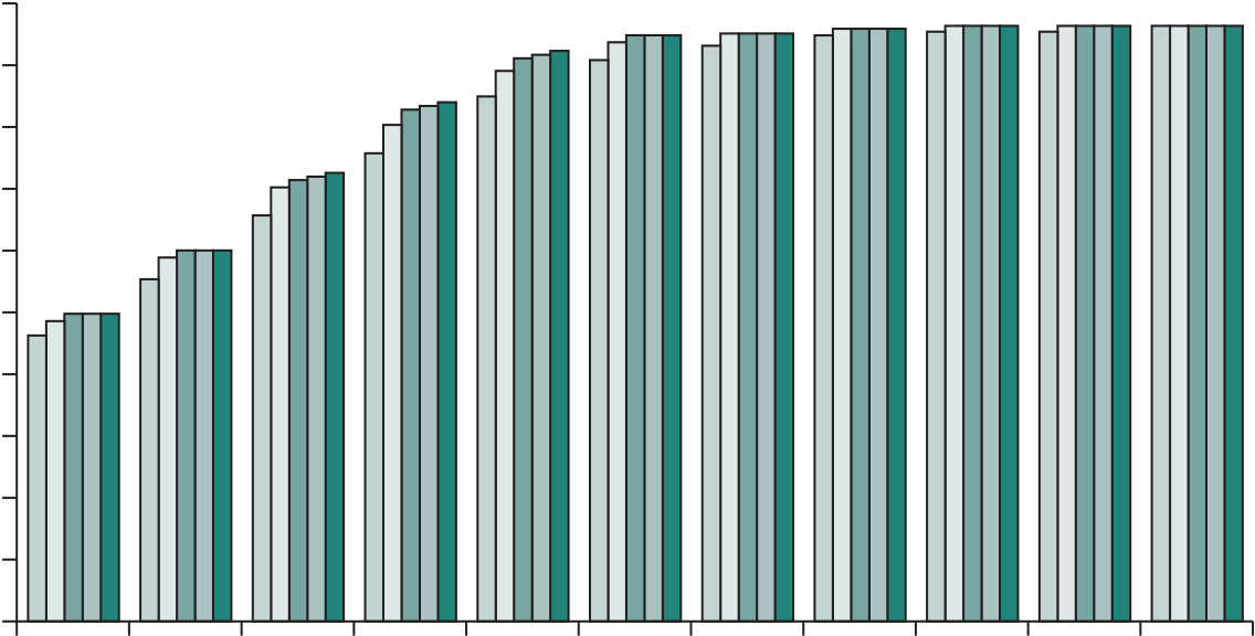
In the extreme case of v = m,k = 1, the set- associative technique reduces to direct mapping, and for v = 1,k = m, it reduces to associative mapping. The use of two lines per set (v = m/2,k = 2) is the most common set- associative organization. It significantly improves the hit ratio over direct mapping. Four- way set associative (v = m/4,k = 4) makes a modest additional improvement for a relatively small additional cost [MAYB84, HILL89]. Further increases in the number of lines per set have little effect.
Figure 4.16 shows the results of one simulation study of set- associative cache performance as a function of cache size [GENU04]. The difference in performance between direct and two- way set associative is significant up to at least a cache size of 64 kB. Note also that the difference between two- way and four- way at 4 kB is much less than the difference in going from for 4 kB to 8 kB in cache size. The complexity of the cache increases in proportion to the associativity, and in this case would not be justifiable against increasing cache size to 8 or even 16 kB. A final point to note is that beyond about 32 kB, increase in cache size brings no significant increase in performance.
Replacement Algorithms
Once the cache has been filled, when a new block is brought into the cache, one of the existing blocks must be replaced. For direct mapping, there is only one possible line for any particular block, and no choice is possible. For the associative and set- associative techniques, a replacement algorithm is needed. To achieve high speed, such an algorithm must be implemented in hardware. A number of algorithms have been tried. We mention four of the most common. Probably the most effective is least recently used (LRU): Replace that block in the set that has been in the cache longest with no reference to it. For two- way set associative, this is easily implemented. Each line includes a USE bit. When a line is referenced, its USE bit is set to 1 and the USE bit of the other line in that set is set to 0. When a block is to be read into the set, the line whose USE bit is 0 is used. Because we are assuming that more recently used memory locations are more likely to be referenced, LRU should give the best hit ratio. LRU is also relatively easy to implement for a fully associative cache. The cache mechanism maintains a separate list of indexes to all the lines in the cache. When a line is referenced, it moves to the front of the list. For replacement, the line at the back of the list is used. Because of its simplicity of implementation, LRU is the most popular replacement algorithm.
146 CHApter 4 / CACHe memory
of this technique is that it generates substantial memory traffic and may create a bot-tleneck. An alternative technique, known as write back, minimizes memory writes. With write back, updates are made only in the cache. When an update occurs, a dirty bit, or use bit, associated with the line is set. Then, when a block is replaced, it is written back to main memory if and only if the dirty bit is set. The problem with write back is that portions of main memory are invalid, and hence accesses by I/O modules can be allowed only through the cache. This makes for complex circuitry and a potential bottleneck. Experience has shown that the percentage of memory references that are writes is on the order of 15% [SMIT82]. However, for HPC applications, this number may approach 33% ( vector- vector multiplication) and can go as high as 50% (matrix transposition).
■ Larger blocks reduce the number of blocks that fit into a cache. Because each block fetch overwrites older cache contents, a small number of blocks results in data being overwritten shortly after they are fetched.
■ As a block becomes larger, each additional word is farther from the requested word and therefore less likely to be needed in the near future.
The inclusion of an on- chip cache leaves open the question of whether an off- chip, or external, cache is still desirable. Typically, the answer is yes, and most contemporary designs include both on- chip and external caches. The simplest such organization is known as a two- level cache, with the internal level 1 (L1) and the external cache designated as level 2 (L2). The reason for including an L2 cache is the following: If there is no L2 cache and the processor makes an access request for a memory location not in the L1 cache, then the processor must access DRAM or
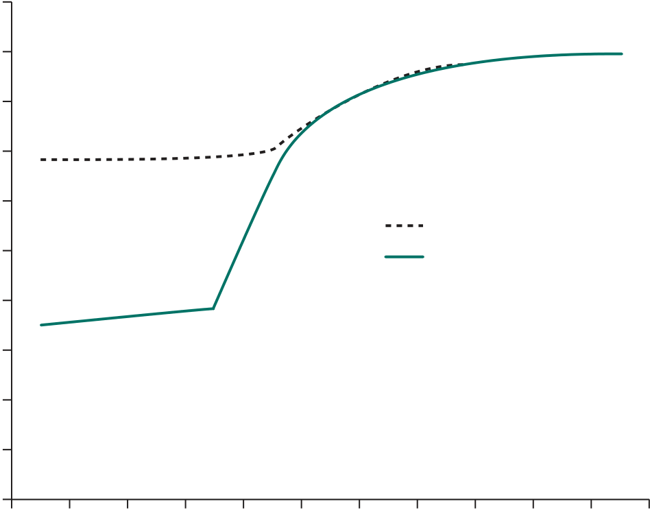
Figure 4.17 shows the results of one simulation study of two- level cache perfor-mance as a function of cache size [GENU04]. The figure assumes that both caches have the same line size and shows the total hit ratio. That is, a hit is counted if the desired data appears in either the L1 or the L2 cache. The figure shows the impact of L2 on total hits with respect to L1 size. L2 has little effect on the total number of cache hits until it is at least double the L1 cache size. Note that the steepest part of the slope for an L1 cache of 8 kB is for an L2 cache of 16 kB. Again for an L1 cache of 16 kB, the steepest part of the curve is for an L2 cache size of 32 kB. Prior to that point, the L2 cache has little, if any, impact on total cache performance. The need for the L2 cache to be larger than
0.98
| 1k | 2k | 4k | 8k | 16k | 32k | 64k | 128k 256k 512k | 1M |
|
|---|
L2 cache size (bytes)
unifiedversussplitcaches When the on- chip cache first made an appearance, many of the designs consisted of a single cache used to store references to both data and instructions. More recently, it has become common to split the cache into two: one dedicated to instructions and one dedicated to data. These two caches both exist at the same level, typically as two L1 caches. When the processor attempts to fetch an instruction from main memory, it first consults the instruction L1 cache, and when the processor attempts to fetch data from main memory, it first consults the data L1 cache.
There are two potential advantages of a unified cache:
The evolution of cache organization is seen clearly in the evolution of Intel micro-processors (Table 4.4). The 80386 does not include an on- chip cache. The 80486 includes a single on- chip cache of 8 kB, using a line size of 16 bytes and a four- way
150 CHApter 4 / CACHe memory
set- associative organization. All of the Pentium processors include two on- chip L1 caches, one for data and one for instructions. For the Pentium 4, the L1 data cache is 16 kB, using a line size of 64 bytes and a four- way set- associative organi-zation. The Pentium 4 instruction cache is described subsequently. The Pentium II also includes an L2 cache that feeds both of the L1 caches. The L2 cache is eight- way set associative with a size of 512 kB and a line size of 128 bytes. An L3 cache was added for the Pentium III and became on- chip with high- end versions of the Pentium 4.
System bus
| Out-of-order | L1 instruction | Instruction |
|---|---|---|
| execution | cache (12K mops) |
|
| logic | unit |
L2 cache
(512 kB)
| L1 data cache (16 kB) | 256 |
|---|
bits
Note: CD = 0; NW = 1 is an invalid combination.
The L1 data cache is controlled by two bits in one of the control registers, labe-led the CD (cache disable) and NW (not write- through) bits (Table 4.5). There are also two Pentium 4 instructions that can be used to control the data cache: INVD invalidates (flushes) the internal cache memory and signals the external cache (if any) to invalidate. WBINVD writes back and invalidates internal cache and then writes back and invalidates external cache.
Both the L2 and L3 caches are eight- way set- associative with a line size of 128 bytes.
|
|---|
4.5 / Key termS, review QueStionS, AnD problemS 153
|
What are the differences among sequential access, direct access, and random access?
|
|---|
154 CHApter 4 / CACHe memory
c. For the two- way set- associative cache example of Figure 4.15: address length, num-ber of addressable units, block size, number of blocks in main memory, number of lines in set, number of sets, number of lines in cache, size of tag
|
||||
|---|---|---|---|---|
| 0001 | 0001 | 0001 |
|
|
| 1100 | 0011 | 0011 |
|
|
| 1101 | 0000 | 0001 | ||
| 1010 | 1010 | 1010 | ||
B1 |
||||||
|---|---|---|---|---|---|---|
|
|
|||||
| Yes | ||||||
| B0 |
||||||
| Yes | No | Yes | No | |||
|
Replace | Replace | Replace | |||
| L1 | L2 | L3 | ||||
Figure 4.19 Intel 80486 On- Chip Cache Replacement Strategy
for (j = 0; j 6 10; j+ +)
a[i] = a[i]*j
| 4.16 4.17 |
|---|
order. It then repeats this fetch sequence nine more times. The cache is 10 times faster than main memory. Estimate the improvement resulting from the use of the cache. Assume an LRU policy for block replacement.
4.20 4.21 |
|
|---|
b. Repeat the calculations assuming insertion of two wait states of one cycle each per memory cycle. What conclusion can you draw from the results?
Ta = Tc + (1- H)Tm
| 4.27 |
|
|
|---|---|---|
| 4.28 | Assume the following performance characteristics on a cache read miss: one clock | |
|
||
| 4.29 | For the cache design of the preceding problem, suppose that increasing the line size | |
|
|
|
The basis for the performance advantage of a two- level memory is a principle known as locality of reference [DENN68]. This principle states that memory references tend to cluster. Over a long period of time, the clusters in use change, but over a short period of time, the processor is primarily working with fixed clusters of mem-ory references.
Intuitively, the principle of locality makes sense. Consider the following line of reasoning:
Table 4.6 Characteristics of Two- Level Memories
|
|||||||||||||||||||||
|---|---|---|---|---|---|---|---|---|---|---|---|---|---|---|---|---|---|---|---|---|---|
A distinction is made in the literature between spatial locality and temporal locality. Spatial locality refers to the tendency of execution to involve a number of memory locations that are clustered. This reflects the tendency of a processor to access instructions sequentially. Spatial location also reflects the tendency of a pro-gram to access data locations sequentially, such as when processing a table of data. Temporal locality refers to the tendency for a processor to access memory locations that have been used recently. For example, when an iteration loop is executed, the processor executes the same set of instructions repeatedly.
w= 5
CallNesting
depth
To express the average time to access an item, we must consider not only the speeds of the two levels of memory, but also the probability that a given reference can be found in M1. We have
Figure 4.2 shows average access time as a function of hit ratio. As can be seen, for a high percentage of hits, the average total access time is much closer to that of M1 than M2.
Performance
We would like Cs ≈ C2. Given that C1 W C2, this requires S1 6 S2. Figure 4.21 shows the relationship.
| 1000 |
|
|---|
| 1 | 5 | 6 | 7 | 2 | 3 | 4 | 5 | 6 | 7 | 2 | 3 | 4 | 5 | 6 | 7 | 8 91000 |
|---|
Relative size of two levels (S2/S1)
Figure 4.21 Relationship of Average Memory Cost to Relative Memory Size for a Two- Level Memory
So we would like M1 to be small to hold down cost, and large to improve the hit ratio and therefore the performance. Is there a size of M1 that satisfies both requirements to a reasonable extent? We can answer this question with a series of subquestions:
■ What value of hit ratio is needed so that Ts ≈ T1?■ What size of M1 will assure the needed hit ratio?
1
r= 1
| Access effciency =T1/Ts | 0.1 | 0.2 | r= 1000 | 0.6 | 0.8 | 1.0 | ||
|---|---|---|---|---|---|---|---|---|
| 0.01 | ||||||||
| 0.001 | ||||||||
Hit ratio =H
Figure 4.22 Access Efficiency as a Function of Hit Ratio (r = T2/T1)
So if there is strong locality, it is possible to achieve high values of hit ratio even with relatively small upper- level memory size. For example, numerous studies have shown that rather small cache sizes will yield a hit ratio above 0.75 regardless of the size of main memory (e.g., [AGAR89], [PRZY88], [STRE83], and [SMIT82]). A cache in the range of 1K to 128K words is generally adequate, whereas main
1.0
0.4
No locality
| 0.2 | 0.4 | 0.6 | 0.8 | 1.0 |
|---|
164 CHApter 4 / CACHe memory
memory is now typically in the gigabyte range. When we consider virtual memory and disk cache, we will cite other studies that confirm the same phenomenon, namely that a relatively small M1 yields a high value of hit ratio because of locality.
Internal MeMory
5.1 Semiconductor Main Memory
Organization
DRAM and SRAM
Types of ROM
Chip Logic
Chip Packaging
Module Organization
Interleaved Memory5.6 Key Terms, Review Questions, and Problems
165
Organization
The basic element of a semiconductor memory is the memory cell. Although a vari-ety of electronic technologies are used, all semiconductor memory cells share certain properties:
5.1 / SeMIConduCtor MaIn MeMory 167
| Select | Control | Select | Control | ||
|---|---|---|---|---|---|
| Cell | Cell | ||||
| (a) Write | (b) Read |
All of the memory types that we will explore in this chapter are random access. That is, individual words of memory are directly accessed through wired-in addressing logic.
Table 5.1 lists the major types of semiconductor memory. The most common is referred to as random-access memory (RAM). This is, in fact, a misuse of the term, because all of the types listed in the table are random access. One distinguishing characteristic of memory that is designated as RAM is that it is possible both to read data from the memory and to write new data into the memory easily and rapidly. Both the reading and writing are accomplished through the use of electrical signals.
168 Chapter 5 / Internal MeMory
dynamic refers to this tendency of the stored charge to leak away, even with power continuously applied.
staticram In contrast, a static RAM (SRAM) is a digital device that uses the same logic elements used in the processor. In a SRAM, binary values are stored using traditional flip-flop logic-gate configurations (see Chapter 11 for a description of flip-flops). A static RAM will hold its data as long as power is supplied to it.
Figure 5.2b is a typical SRAM structure for an individual cell. Four transistors (T1,T2,T3,T4) are cross connected in an arrangement that produces a stable logic
| T5 | T4 | |||
|---|---|---|---|---|
| Transistor |
|
C2 |
Storage
capacitor
Figure 5.2 Typical Memory Cell Structures
5.1 / SeMIConduCtor MaIn MeMory 169
As the name suggests, a read-only memory (ROM) contains a permanent pattern of data that cannot be changed. A ROM is nonvolatile; that is, no power source is required to maintain the bit values in memory. While it is possible to read a ROM, it is not possible to write new data into it. An important application of ROMs is micro-programming, discussed in Part Four. Other potential applications include
■ Library subroutines for frequently wanted functions
■ The data insertion step includes a relatively large fixed cost, whether one or thousands of copies of a particular ROM are fabricated.
■ There is no room for error. If one bit is wrong, the whole batch of ROMs must be thrown out.
Another variation on read-only memory is the read-mostly memory, which is useful for applications in which read operations are far more frequent than write operations but for which nonvolatile storage is required. There are three common forms of read-mostly memory: EPROM, EEPROM, and flash memory.
The optically erasable programmable read-only memory (EPROM) is read and written electrically, as with PROM. However, before a write operation, all the stor-age cells must be erased to the same initial state by exposure of the packaged chip to ultraviolet radiation. Erasure is performed by shining an intense ultraviolet light through a window that is designed into the memory chip. This erasure process can be performed repeatedly; each erasure can take as much as 20 minutes to perform. Thus, the EPROM can be altered multiple times and, like the ROM and PROM, holds its data virtually indefinitely. For comparable amounts of storage, the EPROM is more expensive than PROM, but it has the advantage of the multiple update capability.
In the memory hierarchy as a whole, we saw that there are trade-offs among speed, density, and cost. These trade-offs also exist when we consider the organiza-tion of memory cells and functional logic on a chip. For semiconductor memories, one of the key design issues is the number of bits of data that may be read/written at a time. At one extreme is an organization in which the physical arrangement of cells in the array is the same as the logical arrangement (as perceived by the pro-cessor) of words in memory. The array is organized into W words of B bits each.
An additional 11 address lines select one of 2048 columns of 4 bits per column. Four data lines are used for the input and output of 4 bits to and from a data buffer. On input (write), the bit driver of each bit line is activated for a 1 or 0 according to the value of the corresponding data line. On output (read), the value of each bit line is passed through a sense amplifier and presented to the data lines. The row line selects which row of cells is used for reading or writing.
RAS CAS WE OE
172 Chapter 5 / Internal MeMory
Because only 4 bits are read/written to this DRAM, there must be multiple DRAMs connected to the memory controller to read/write a word of data to the bus.
Chip Packaging
As was mentioned in Chapter 2, an integrated circuit is mounted on a package that contains pins for connection to the outside world.
■ A ground pin (Vss).
■ A chip enable (CE) pin. Because there may be more than one memory chip, each of which is connected to the same address bus, the CE pin is used to indi-cate whether or not the address is valid for this chip. The CE pin is activated by logic connected to the higher-order bits of the address bus (i.e., address bits above A19). The use of this signal is illustrated presently.
|
1 | 32 | Vcc | Vcc | 1 | 24 | Vss | ||||
|---|---|---|---|---|---|---|---|---|---|---|---|
|
2 | 31 | A18 | D0 | 2 | 23 | D3 | ||||
| 3 | 30 | A17 | D1 | 3 | 22 | D2 | |||||
| 4 | 29 | A14 | WE | 4 | 21 | CAS | |||||
| A7 | 5 | 28 | A13 | RAS | 5 | 20 | OE | ||||
| A6 | 6 | 27 | A8 | NC | 6 | 24-Pin Dip | A9 | ||||
| A5 | 7 | 26 | A9 | A10 | 7 | 0.6" | A8 | ||||
| A4 | 8 | 25 | A11 | A0 | 8 | 17 | A7 | ||||
| A3 | 9 | 32-Pin Dip |
|
Vpp | A1 | 9 | 16 | A6 | |||
| A2 | 10 | 0.6" |
|
A10 | A2 | 10 | 15 | A5 | |||
| A1 | 11 | CE | A3 | 11 | 14 | A4 | |||||
| A0 | 12 | 21 | D7 | Vcc | 12 | Top View | Vss | ||||
| D0 | 13 | 20 | D6 | (b) 16-Mbit DRAM | |||||||
| D1 | 14 | 19 | D5 | ||||||||
| D2 | 15 | 18 | D4 | ||||||||
| 16 | Top View | D3 | |||||||||
| (a) 8-Mbit EPROM | |||||||||||
Figure 5.4 Typical Memory Package Pins and Signals
Because the DRAM is accessed by row and column, and the address is multi-plexed, only 11 address pins are needed to specify the 4M row/column combinations (211* 211= 222= 4M). The functions of the row address select (RAS) and col-umn address select (CAS) pins were discussed previously. Finally, the no connect (NC) pin is provided so that there are an even number of pins.
Main memory is composed of a collection of DRAM memory chips. A number of chips can be grouped together to form a memory bank. It is possible to organize the memory
| 9 | • | Decode 1 of | Memory buffer | |
|---|---|---|---|---|
| 512 bit-sense | ||||
| 9 | • | register (MBR) | ||
| • | 1 | |||
| 2 | ||||
8
Decode 1 of
512 bit-sense
5.2 error correction
A semiconductor memory system is subject to errors. These can be categorized as hard failures and soft errors. A hard failure is a permanent physical defect so that the memory cell or cells affected cannot reliably store data but become stuck at 0 or 1 or
| E |
|
E | 1/512 | B1 | E |
|
D1 | Memory | |||
|---|---|---|---|---|---|---|---|---|---|---|---|
| 9 | 1/512 | 1/512 | E | buffer | |||||||
| register | |||||||||||
| (MBR) | |||||||||||
| 9 | E | A2 | E |
|
|
1 | |||||
| 2 | |||||||||||
| 2 | |||||||||||
| 7 | |||||||||||
| D7 | |||||||||||
| 1/512 | |||||||||||
| 8 | |||||||||||
| Group | |||||||||||
|
|
E | |||||||||
| D8 | |||||||||||
|
E | ||||||||||
| 1/512 | 1/512 | ||||||||||
|
E | ||||||||||
Figure 5.7 illustrates in general terms how the process is carried out. When data are to be written into memory, a calculation, depicted as a function f, is per-formed on the data to produce a code. Both the code and the data are stored. Thus, if an M-bit word of data is to be stored and the code is of length K bits, then the actual size of the stored word is M + K bits.
When the previously stored word is read out, the code is used to detect and possibly correct errors. A new set of K code bits is generated from the M data bits and compared with the fetched code bits. The comparison yields one of three results:
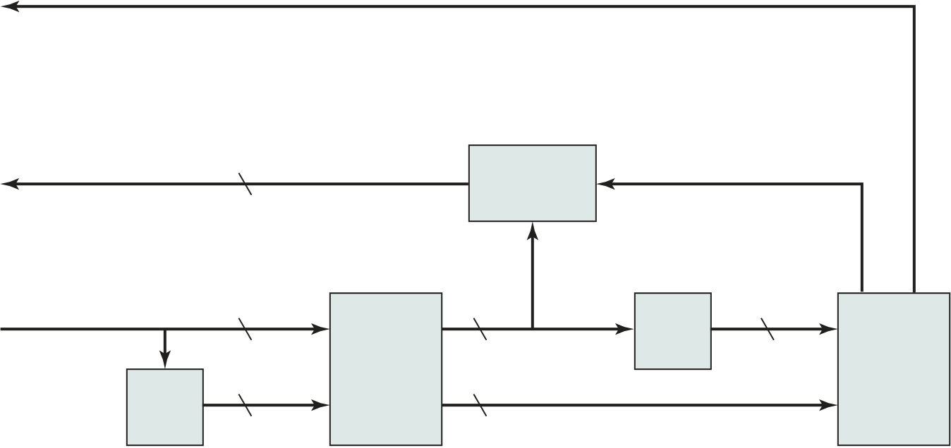
176 Chapter 5 / Internal MeMory
| K | Memory | Compare |
|---|
f
Figure 5.7 Error-Correcting Code Function
2K-1 Ú M + K
This inequality gives the number of bits needed to correct a single bit error in a word containing M data bits. For example, for a word of 8 data bits (M = 8), we have
| (c) | 1 | 0 | 1 | 0 | (d) | 1 | 0 | 1 | 0 | ||
|---|---|---|---|---|---|---|---|---|---|---|---|
| 1 | 1 | ||||||||||
| 0 | 0 |
Figure 5.8 Hamming Error-Correcting Code
Thus, eight data bits require four check bits. The first three columns of Table 5.2 lists the number of check bits required for various data word lengths.
To achieve these characteristics, the data and check bits are arranged into a 12-bit word as depicted in Figure 5.9. The bit positions are numbered from 1 to 12. Those bit positions whose position numbers are powers of 2 are designated as check
178 Chapter 5 / Internal MeMory
Each check bit operates on every data bit whose position number contains a 1 in the same bit position as the position number of that check bit. Thus, data bit pos-itions 3, 5, 7, 9, and 11 (D1, D2, D4, D5, D7) all contain a 1 in the least significant bit of their position number as does C1; bit positions 3, 6, 7, 10, and 11 all contain a 1 in is checked by those bits Ci such that a i = n. For example, position 7 is checked by bits in position 4, 2, and 1; and 7 = 4 + 2 + 1.
Let us verify that this scheme works with an example. Assume that the 8-bit input word is 00111001, with data bit D1 in the rightmost position. The calculations are as follows:
| 12 | 11 | 10 | 9 | 8 | 7 | 6 | 5 | 4 | 3 | 2 | 1 | |
|---|---|---|---|---|---|---|---|---|---|---|---|---|
| 1100 | 1011 | 1010 | 1001 | 1000 | 0111 | 0110 | 0101 | 0100 | 0011 | 0010 | 0001 | |
| D8 | D7 | D6 | D5 | D4 | D3 | D2 | D1 | |||||
| Check bit | C8 | C4 | C2 | C1 |
Figure 5.9 Layout of Data Bits and Check Bits

C4 = 0 ⊕ 1 ⊕ 1 ⊕ 0 = 0
C8 = 1 ⊕ 1 ⊕ 0 ⊕ 0 = 0
The code just described is known as a single-error-correcting (SEC) code. More commonly, semiconductor memory is equipped with a single-error-correcting, double-error-detecting (SEC-DED) code. As Table 5.2 shows, such codes require one additional bit compared with SEC codes.
Figure 5.11 illustrates how such a code works, again with a 4-bit data word. The sequence shows that if two errors occur (Figure 5.11c), the checking procedure goes astray (d) and worsens the problem by creating a third error (e). To overcome
| 12 | 11 | 10 | 9 | 8 | 7 | 6 | 5 | 4 | 3 | 2 | 1 | |
|---|---|---|---|---|---|---|---|---|---|---|---|---|
| 1100 | 1011 | 1010 | 1001 | 1000 | 0111 | 0110 | 0101 | 0100 | 0011 | 0010 | 0001 | |
|
D8 | D7 | D6 | D5 | C8 | D4 | D3 | D2 | C4 | D1 | C2 | C1 |
| Check bit | ||||||||||||
|
0 | 0 | 1 | 1 | 0 | 1 | 0 | 0 | 1 | 1 | 1 | 1 |
| 0 | 0 | 1 | 1 | 0 | 1 | 1 | 0 | 1 | 1 | 1 | 1 | |
| 1100 | 1011 | 1010 | 1001 | 1000 | 0111 | 0110 | 0101 | 0100 | 0011 | 0010 | 0001 | |
| Check bit | 0 | 0 | 0 | 1 |
180 Chapter 5 / Internal MeMory
Figure 5.11 Hamming SEC-DEC Code
the problem, an eighth bit is added that is set so that the total number of 1s in the diagram is even. The extra parity bit catches the error (f).
In recent years, a number of enhancements to the basic DRAM architecture have been explored. The schemes that currently dominate the market are SDRAM and DDR-DRAM. We examine each of these in turn.
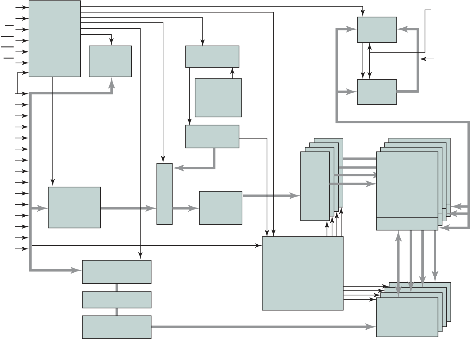
With synchronous access, the DRAM moves data in and out under control of the system clock. The processor or other master issues the instruction and address information, which is latched by the DRAM. The DRAM then responds after a set number of clock cycles. Meanwhile, the master can safely do other tasks while the SDRAM is processing the request.
Figure 5.12 shows the internal logic of a typical 256-Mb SDRAM typical of SDRAM organization, and Table 5.3 defines the various pin assignments. The
|
13 |
|
Data in | ||||||||||
|---|---|---|---|---|---|---|---|---|---|---|---|---|---|
| CS | DQ 0-15 | ||||||||||||
| 16 | buffer | 16 | |||||||||||
|
|||||||||||||
| clock | |||||||||||||
|
|||||||||||||
|
Row | 13 | Self- | Data out | |||||||||
| refresh | 16 | buffer |
|
||||||||||
| controller | |||||||||||||
|
Memory cell array | ||||||||||||
|
|||||||||||||
| Row | |||||||||||||
|
8192 | (4 Mb x 16) | |||||||||||
|
|||||||||||||
| DRAM | |||||||||||||
| address | address | BANK 0 | |||||||||||
| 13 | latch | 13 | |||||||||||
| Sense amps | |||||||||||||
BA0
| Column | 9 | |
|---|---|---|
Figure 5.12 256-Mb Synchronous Dynamic RAM (SDRAM)
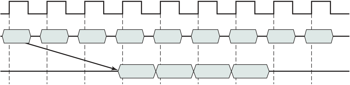
The mode register and associated control logic is another key feature differen-tiating SDRAMs from conventional DRAMs. It provides a mechanism to custom-ize the SDRAM to suit specific system needs. The mode register specifies the burst length, which is the number of separate units of data synchronously fed onto the bus. The register also allows the programmer to adjust the latency between receipt of a read request and the beginning of data transfer.
The SDRAM performs best when it is transferring large blocks of data sequen-tially, such as for applications like word processing, spreadsheets, and multimedia.
| T0 | T1 | T2 | T3 | T4 | T5 | T6 | T7 | T8 |
|---|
Although SDRAM is a significant improvement on asynchronous RAM, it still has shortcomings that unnecessarily limit that I/O data rate that can be achieved. To address these shortcomings a newer version of SDRAM, referred to as double- data-rate DRAM (DDR DRAM) provides several features that dramatically increase the data rate. DDR DRAM was developed by the JEDEC Solid State Tech-nology Association, the Electronic Industries Alliance’s semiconductor-engineering- standardization body. Numerous companies make DDR chips, which are widely used in desktop computers and servers.
DDR achieves higher data rates in three ways. First, the data transfer is syn-chronized to both the rising and falling edge of the clock, rather than just the rising edge. This doubles the data rate; hence the term double data rate. Second, DDR uses higher clock rate on the bus to increase the transfer rate. Third, a buffering scheme is used, as explained subsequently.
| DDR1 | DDR2 | DDR3 | DDR4 | |
|---|---|---|---|---|
|
2 | 4 | 8 | 8 |
|
2.5 | 1.8 | 1.5 | 1.2 |
| 200—400 | 400—1066 | 800—2133 | 2133—4266 |
100–150 Mbps
| 2N | MUX | DDR | ||
|---|---|---|---|---|
Memory array (100–266 MHz)
Figure 5.14 shows a configuration with two bank groups. With DDR4, up to 4 bank groups can be used.
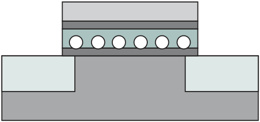
Operation
Figure 5.15 illustrates the basic operation of a flash memory. For comparison, Fig-ure 5.15a depicts the operation of a transistor. Transistors exploit the properties of semiconductors so that a small voltage applied to the gate can be used to control the flow of a large current between the source and the drain.
| Control gate | |||||
|---|---|---|---|---|---|
|
P-substrate | ||||
| P-substrate | |||||
| + | + + | + + | |||||
|---|---|---|---|---|---|---|---|
| Control gate | |||||||
| – | – | – | – | – | |||
| N+ | N+ | ||||||
| Drain | Source | ||||||
Figure 5.15 Flash Memory Operation
Although the specific quantitative values of various characteristics of NOR and NAND are changing year by year, the relative differences between the two types has remained stable. These differences are usefully illustrated by the Kiviat graphs3 shown in Figure 5.17.
Bit line
Bit line
| Ground | Word | Word | Word | Word | Word | Word | Word |
|
|
|---|---|---|---|---|---|---|---|---|---|
| select | |||||||||
| transistor | line 0 | line 1 | line 2 | line 3 | line 4 | line 5 | line 6 | line 7 |
(b) NAND fash structure
Figure 5.16 Flash Memory Structures
5.5 newer nonvolatile Solid-State memory technologieS
The traditional memory hierarchy has consisted of three levels (Figure 5.18):
188 Chapter 5 / Internal MeMory
Increasing performance
and endurance
| SRAM |
|---|
ReRAM
HARD DISK
Recently, there have been breakthroughs in developing new forms of non-volatile semiconductor memory that continue scaling beyond flash memory. The most promising technologies are spin-transfer torque RAM (STT-RAM), phase-change RAM (PCRAM), and resistive RAM (ReRAM) ([ITRS14], [GOER12]). All of these are in volume production. However, because NAND Flash and to some extent NOR Flash are still dominating the applications, these emerging memories have been used in specialty applications and have not yet fulfilled their original promise to become dominating mainstream high-density nonvolatile memory. This is likely to change in the next few years.
Figure 5.18 shows how these three technologies are likely to fit into the mem-ory hierarchy.
Phase-change RAM (pcram) is the most mature or the new technologies, with an extensive technical literature ([RAOU09], [ZHOU09], [LEE10]).
PCRAM technology is based on a chalcogenide alloy material, which is similar to those commonly used in optical storage media (compact discs and digital versa-tile discs). The data storage capability is achieved from the resistance differences between an amorphous (high-resistance) and a crystalline (low-resistance) phase of the chalcogenide-based material. In SET operation, the phase change material is crystallized by applying an electrical pulse that heats a significant portion of the cell above its crystallization temperature. In RESET operation, a larger electrical current is applied and then abruptly cut off in order to melt and then quench the material, leaving it in the amorphous state. Figure 5.19b illustrates the general configuration.
190 Chapter 5 / Internal MeMory
(a) STT-RAM
| Top electrode | Polycrystaline | Top electrode | Polycrystaline | |
|---|---|---|---|---|
| chalcogenide | ||||
| Bottom electrode | Bottom electrode | |||
|
||||
|
|
|
|---|
Review Questions
|
|---|
| Row address |
|
|
|---|---|---|
|
5.8 5.9 |
|
|---|
5.6 / Key terMS, revIew QueStIonS, and probleMS 193
(b) Truth table
A0
A1
A2
A3
CS
| n | m | l | k | j | i | h | g | f | e | d | c | b | a |
|---|
|
|
|---|


CHAPTER
6.4 Optical Memory
Compact Disk
Digital Versatile Disk
High- Definition Optical Disks6.5 Magnetic Tape
This chapter examines a range of external memory devices and systems. We begin with the most important device, the magnetic disk. Magnetic disks are the founda-tion of external memory on virtually all computer systems. The next section exam-ines the use of disk arrays to achieve greater performance, looking specifically at the family of systems known as RAID (Redundant Array of Independent Disks). An increasingly important component of many computer systems is the solid state disk, which is discussed next. Then, external optical memory is examined. Finally, magnetic tape is described.
6.1 MAGNETIC DISK
■ Better stiffness to reduce disk dynamics.
■ Greater ability to withstand shock and damage.
196 cHaPteR 6 / exteRnal MeMoRy
Read
current
| Write current |
|---|
Recording
medium
Figure 6.1 Inductive Write/Magnetoresistive Read Head
The head is a relatively small device capable of reading from or writing to a portion of the platter rotating beneath it. This gives rise to the organization of data on the platter in a concentric set of rings, called tracks. Each track is the same width as the head. There are thousands of tracks per surface.
Inter-sector gap
Track sector
| Cylinder | Direction of |
|
|
|---|---|---|---|
| arm motion |
Figure 6.2 Disk Data Layout
Track
Figure 6.3 Comparison of Disk Layout Methods
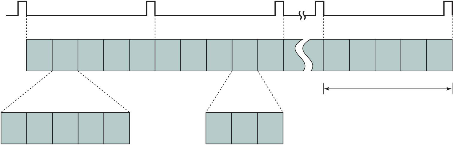
Table 6.1 lists the major characteristics that differentiate among the various types of magnetic disks. First, the head may either be fixed or movable with respect to the radial direction of the platter. In a fixed- head disk, there is one read- write head per track. All of the heads are mounted on a rigid arm that extends across all tracks; such systems are rare today. In a movable- head disk, there is only one read- write head. Again, the head is mounted on an arm. Because the head must be able to be positioned above any track, the arm can be extended or retracted for this purpose.
The disk itself is mounted in a disk drive, which consists of the arm, a spindle that rotates the disk, and the electronics needed for input and output of binary data. A nonremovable disk is permanently mounted in the disk drive; the hard disk in a personal computer is a nonremovable disk. A removable disk can be removed and replaced with another disk. The advantage of the latter type is that unlimited amounts of data are available with a limited number of disk systems. Furthermore, such a disk may be moved from one computer system to another. Floppy disks and ZIP cartridge disks are examples of removable disks.
600 bytes/sector
Figure 6.4 Winchester Disk Format (Seagate ST506)
200 cHaPteR 6 / exteRnal MeMoRy
|
|---|
For most disks, the magnetizable coating is applied to both sides of the plat-ter, which is then referred to as double sided. Some less expensive disk systems use single- sided disks.
Some disk drives accommodate multiple platters stacked vertically a fraction of an inch apart. Multiple arms are provided (Figure 6.2). Multiple– platter disks employ a movable head, with one read- write head per platter surface. All of the heads are mechanically fixed so that all are at the same distance from the center of the disk and move together. Thus, at any time, all of the heads are positioned over tracks that are of equal distance from the center of the disk. The set of all the tracks in the same relative position on the platter is referred to as a cylinder. This is illus-trated in Figure 6.2.
Table 6.2 Typical Hard Disk Drive Parameters
The actual details of disk I/O operation depend on the computer system, the oper-ating system, and the nature of the I/O channel and disk controller hardware. A general timing diagram of disk I/O transfer is shown in Figure 6.5.
When the disk drive is operating, the disk is rotating at constant speed. To read or write, the head must be positioned at the desired track and at the beginning of the desired sector on that track. Track selection involves moving the head in a movable- head system or electronically selecting one head on a fixed- head system. On a movable- head system, the time it takes to position the head at the track is known as seek time. In either case, once the track is selected, the disk controller waits until the appropriate sector rotates to line up with the head. The time it takes for the beginning of the sector to reach the head is known as rotational delay, or rotational latency. The sum of the seek time, if any, and the rotational delay equals the access time, which is the time it takes to get into position to read or write. Once the head is in position, the read or write operation is then performed as the sector moves under the head; this is the data transfer portion of the operation; the time required for the transfer is the transfer time.
| Wait for | Wait for | Seek | Rotational | Data |
|---|---|---|---|---|
| device | channel | delay | transfer |
In some high- end systems for servers, a technique known as rotational pos-itional sensing (RPS) is used. This works as follows: When the seek command has been issued, the channel is released to handle other I/O operations. When the seek is completed, the device determines when the data will rotate under the head. As that sector approaches the head, the device tries to reestablish the communication path back to the host. If either the control unit or the channel is busy with another I/O, then the reconnection attempt fails and the device must rotate one whole revolution before it can attempt to reconnect, which is called an RPS miss. This is an extra delay element that must be added to the timeline of Figure 6.5.
seektime Seek time is the time required to move the disk arm to the required track. It turns out that this is a difficult quantity to pin down. The seek time consists of two key components: the initial startup time, and the time taken to traverse the tracks that have to be crossed once the access arm is up to speed. Unfortunately, the traversal time is not a linear function of the number of tracks, but includes a settling time (time after positioning the head over the target track until track identification is confirmed).
| T | b |
|---|---|
| = | rN |
T = transfertime
b = numberof bytes to be transferred
N = numberof bytes on a track
r = rotationspeed, in revolutions per second
Thus the total average read or write time Ttotal can be expressed as
atimingcomparison With the foregoing parameters defined, let us look at two different I/O operations that illustrate the danger of relying on average values. Consider a disk with an advertised average seek time of 4 ms, rotation speed of 15,000 rpm, and 512-byte sectors with 500 sectors per track. Suppose that we wish to read a file consisting of 2500 sectors for a total of 1.28 Mbytes. We would like to estimate the total time for the transfer.
First, let us assume that the file is stored as compactly as possible on the disk. That is, the file occupies all of the sectors on 5 adjacent tracks (5tracks * 500sectors/track = 2500sectors). This is known as sequential organ-ization. Now, the time to read the first track is as follows:
Totaltime = 10 + (4 * 6) = 34ms = 0.034seconds
Now let us calculate the time required to read the same data using random access rather than sequential access; that is, accesses to the sectors are distributed randomly over the disk. For each sector, we have
|
 |
|---|
RAID Simulator
With the use of multiple disks, there is a wide variety of ways in which the data can be organized and in which redundancy can be added to improve reliability. This could make it difficult to develop database schemes that are usable on a number of platforms and operating systems. Fortunately, industry has agreed on a standard-ized scheme for multiple- disk database design, known as RAID (Redundant Array of Independent Disks). The RAID scheme consists of seven levels,2 zero through six. These levels do not imply a hierarchical relationship but designate different design architectures that share three common characteristics:
1. RAID is a set of physical disk drives viewed by the operating system as a single logical drive.
2Additional levels have been defined by some researchers and some companies, but the seven levels described in this section are the ones universally agreed on.
3In that paper, the acronym RAID stood for Redundant Array of Inexpensive Disks. The term inexpen-sive was used to contrast the small relatively inexpensive disks in the RAID array to the alternative, a single large expensive disk (SLED). The SLED is essentially a thing of the past, with similar disk technol-ogy being used for both RAID and non- RAID configurations. Accordingly, the industry has adopted the term independent to emphasize that the RAID array creates significant performance and reliability gains.
RAID level 0 is not a true member of the RAID family because it does not include redundancy to improve performance. However, there are a few applications, such as some on supercomputers in which performance and capacity are primary concerns and low cost is more important than improved reliability.
For RAID 0, the user and system data are distributed across all of the disks in the array. This has a notable advantage over the use of a single large disk: If two- different I/O requests are pending for two different blocks of data, then there is a good chance that the requested blocks are on different disks. Thus, the two requests can be issued in parallel, reducing the I/O queuing time.
|
strip 1 | strip 2 |
|
|---|---|---|---|
| strip 5 | strip 6 | ||
| strip 9 | strip 10 | ||
|
strip 13 | strip 14 |
|
(b) RAID 1 (Mirrored)
| b1 | b2 | b3 | f0(b) | f1(b) | f2(b) |
|---|
The second requirement is that the application must make I/O requests that drive the disk array efficiently. This requirement is met if the typical request is for large amounts of logically contiguous data, compared to the size of a strip. In this case, a single I/O request involves the parallel transfer of data from multiple disks, increasing the effective transfer rate compared to a single- disk transfer.
raid 0 forhighi/orequestrate In a transaction- oriented environment, the user is typically more concerned with response time than with transfer rate. For an individual I/O request for a small amount of data, the I/O time is dominated by the motion of the disk heads (seek time) and the movement of the disk (rotational latency).
| block 0 | block 1 | block 2 | block 3 |
|
|---|---|---|---|---|
| block 4 | block 5 | block 6 | block 7 |
|
| block 8 | block 9 | block 10 | block 11 | |
| block 12 | block 13 | block 14 | block 15 |
| block 0 | block 1 | block 2 | block 3 | P(0–3) | Q(0–3) |
|---|---|---|---|---|---|
| block 4 | block 5 | block 6 | P(4–7) | Q(4–7) | block 7 |
| block 8 | block 9 | P(8–11) | Q(8–11) | block 10 | block 11 |
| block 12 | P(12–15) | Q(12–15) | block 13 | block 14 | block 15 |
Figure 6.6 RAID Levels (Continued )
multiple I/O requests outstanding. This, in turn, implies that there are multiple inde-pendent applications or a single transaction- oriented application that is capable of multiple asynchronous I/O requests. The performance will also be influenced by the strip size. If the strip size is relatively large, so that a single I/O request only involves a single disk access, then multiple waiting I/O requests can be handled in parallel, reducing the queuing time for each request.
| Physical | Physical | Physical | Physical | |
|---|---|---|---|---|
| disk 0 | disk 1 | disk 2 | disk 3 |
strip 7
strip 14
strip 15
1. A read request can be serviced by either of the two disks that contains the requested data, whichever one involves the minimum seek time plus rota-tional latency.
2. A write request requires that both corresponding strips be updated, but this can be done in parallel. Thus, the write performance is dictated by the slower of the two writes (i.e., the one that involves the larger seek time plus rotational latency). However, there is no “write penalty” with RAID 1. RAID levels 2 through 6 involve the use of parity bits. Therefore, when a single strip is updated, the array management software must first compute and update the parity bits as well as updating the actual strip in question.
RAID Level 2
RAID levels 2 and 3 make use of a parallel access technique. In a parallel access array, all member disks participate in the execution of every I/O request. Typically, the spindles of the individual drives are synchronized so that each disk head is in the same position on each disk at any given time.
RAID 3 is organized in a similar fashion to RAID 2. The difference is that RAID 3 requires only a single redundant disk, no matter how large the disk array. RAID 3 employs parallel access, with data distributed in small strips. Instead of an error- correcting code, a simple parity bit is computed for the set of individual bits in the same position on all of the data disks.
redundancy In the event of a drive failure, the parity drive is accessed and data is reconstructed from the remaining devices. Once the failed drive is replaced, the missing data can be restored on the new drive and operation resumed.
Suppose that drive X1 has failed. If we add X4(i)⊕X1(i) to both sides of the preceding equation, we get
X1(i) = X4(i)⊕X3(i)⊕X2(i)⊕X0(i)
RAID levels 4 through 6 make use of an independent access technique. In an inde-pendent access array, each member disk operates independently, so that separate I/O requests can be satisfied in parallel. Because of this, independent access arrays are more suitable for applications that require high I/O request rates and are rela-tively less suited for applications that require high data transfer rates.
As in the other RAID schemes, data striping is used. In the case of RAID 4 through 6, the strips are relatively large. With RAID 4, a bit- by- bit parity strip is calculated across corresponding strips on each data disk, and the parity bits are stored in the corresponding strip on the parity disk.
212 cHaPteR 6 / exteRnal MeMoRy
The preceding set of equations is derived as follows. The first line shows that a change in X1 will also affect the parity disk X4. In the second line, we add the terms ⊕X1(i)⊕X1(i)]. Because the exclusive- OR of any quantity with itself is 0, this does not affect the equation. However, it is a convenience that is used to create the third line, by reordering. Finally, Equation (6.2) is used to replace the first four terms by X4(i).
RAID 5 is organized in a similar fashion to RAID 4. The difference is that RAID 5 distributes the parity strips across all disks. A typical allocation is a round- robin scheme, as illustrated in Figure 6.6f. For an n- disk array, the parity strip is on a differ-ent disk for the first n stripes, and the pattern then repeats.
The distribution of parity strips across all drives avoids the potential I/O bottle- neck found in RAID 4.
Table 6.4 is a comparative summary of the seven levels.
6.3 SOLID STATE DRIVES
| Level | Advantages | Disadvantages | Applications |
|---|---|---|---|
|
|
||
|
|
||
|
|||
|
|
||
|
|
||
|
|||
|
214 cHaPteR 6 / exteRnal MeMoRy
state refers to electronic circuitry built with semiconductors. An SSD is a memory device made with solid state components that can be used as a replacement to a hard disk drive. The SSDs now on the market and coming on line use NAND flash memory, which is described in Chapter 5.
■ Durability: Less susceptible to physical shock and vibration.
■ Longer lifespan: SSDs are not susceptible to mechanical wear.
SSD Organization
Figure 6.8 illustrates a general view of the common architectural system component associated with any SSD system. On the host system, the operating system invokes file system software to access data on the disk. The file system, in turn, invokes I/O driver software. The I/O driver software provides host access to the particular SSD product. The interface component in Figure 6.8 refers to the physical and electrical interface between the host processor and the SSD peripheral device. If the device is an internal hard drive, a common interface is PCIe. For external devices, one com-mon interface is USB.
Host system
Operating system
software
Controller
Addressing
Flash
memory
components
Figure 6.8 Solid State Drive Architecture
216 cHaPteR 6 / exteRnal MeMoRy
■ Error correction: Logic for error detection and correction.
2. Before the block can be written back to flash memory, the entire block of flash memory must be erased— it is not possible to erase just one page of the flash memory.
3. The entire block from the buffer is now written back to the flash memory.
In 1983, one of the most successful consumer products of all time was introduced: the compact disk (CD) digital audio system. The CD is a nonerasable disk that can store more than 60 minutes of audio information on one side. The huge commercial success of the CD enabled the development of low- cost optical- disk storage technol-ogy that has revolutionized computer data storage. A variety of optical- disk systems have been introduced (Table 6.6). We briefly review each of these.
Compact Disk
|
|---|
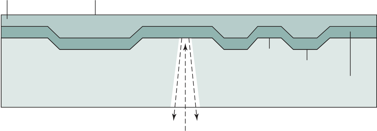
218 cHaPteR 6 / exteRnal MeMoRy
■ Sync: The sync field identifies the beginning of a block. It consists of a byte of all 0s, 10 bytes of all 1s, and a byte of all 0s.
■ Header: The header contains the block address and the mode byte. Mode 0 specifies a blank data field; mode 1 specifies the use of an error- correcting
| Aluminum |
|---|
Laser transmit/
receiveFigure 6.9 CD Operation
| 12 bytes | 4 bytes | 2048 bytes | 288 bytes |
|---|---|---|---|
| SYNC | ID | Data | L-ECC |
Figure 6.10 CD- ROM Block Format
code and 2048 bytes of data; mode 2 specifies 2336 bytes of user data with no error- correcting code.
■ The optical disk together with the information stored on it can be mass repli-cated inexpensively— unlike a magnetic disk. The database on a magnetic disk has to be reproduced by copying one disk at a time using two disk drives.
■ The optical disk is removable, allowing the disk itself to be used for archi-val storage. Most magnetic disks are nonremovable. The information on non-removable magnetic disks must first be copied to another storage medium before the disk drive/disk can be used to store new information.
The CD- R medium is similar to but not identical to that of a CD or CD- ROM. For CDs and CD- ROMs, information is recorded by the pitting of the surface
220 cHaPteR 6 / exteRnal MeMoRy
Digital Versatile Disk
With the capacious digital versatile disk (DVD), the electronics industry has at last found an acceptable replacement for the analog VHS video tape. The DVD has replaced the videotape used in video cassette recorders (VCRs) and, more import-ant for this discussion, replaced the CD- ROM in personal computers and servers. The DVD takes video into the digital age. It delivers movies with impressive picture quality, and it can be randomly accessed like audio CDs, which DVD machines can also play. Vast volumes of data can be crammed onto the disk, currently seven times as much as a CD- ROM. With DVD’s huge storage capacity and vivid quality, PC games have become more realistic and educational software incorporates more video. Following in the wake of these developments has been a new crest of traffic over the Internet and corporate intranets, as this material is incorporated into Web sites.
6.4 / oPtical MeMoRy 221 Label
Laser focuses on polycarbonate
pits in front of refective layer(a) CD-ROM–Capacity 682 MB
| Fully refective layer, side 1 Polycarbonate layer, side 1 |
|---|
(b) DVD-ROM, double-sided, dual-layer–Capacity 17 GB
Figure 6.11 CD- ROM and DVD- ROM
Two competing disk formats and technologies initially competed for market acceptance: HD DVD and Blu- ray DVD. The Blu- ray scheme ultimately achieved market dominance. The HD DVD scheme can store 15 GB on a single layer on a single side. Blu- ray positions the data layer on the disk closer to the laser (shown on the right- hand side of each diagram in Figure 6.12). This enables a tighter focus and less distortion and thus smaller pits and tracks. Blu- ray can store 25 GB on a single layer. Three versions are available: read only ( BD- ROM), recordable once ( BD- R), and rerecordable ( BD- RE).
| DVD | 0.1 µm |
|---|
650 nm
Figure 6.12 Optical Memory Characteristics
6.5 / Magnetic taPe 223
the heads are repositioned to record a new track, and the tape is again recorded on its whole length, this time in the opposite direction. That process continues, back and forth, until the tape is full (Figure 6.13a). To increase speed, the read- write head is capable of reading and writing a number of adjacent tracks simultaneously (typ-ically two to eight tracks). Data are still recorded serially along individual tracks, but blocks in sequence are stored on adjacent tracks, as suggested by Figure 6.13b.
Track 1
Track 0
Figure 6.13 Typical Magnetic Tape Features
224 cHaPteR 6 / exteRnal MeMoRy
| LTO- 1 | LTO- 2 | LTO- 3 | LTO- 4 | LTO- 5 | LTO- 6 | LTO- 7 | LTO- 8 | |
|---|---|---|---|---|---|---|---|---|
| 2000 | 2003 | 2005 | 2007 | 2010 | 2012 | TBA | TBA | |
| 200 GB | 400 GB | 800 GB | 1600 GB | 3.2 TB | 8 TB | 16 TB | 32 TB | |
| Compressed transfer rate |
|
|
|
|||||
|
4880 | 7398 | 9638 | 13,250 | 15,142 | 15,143 | ||
| 384 | 512 | 704 | 896 | 1280 | 2176 | |||
| Tape length (m) | 609 | 609 | 680 | 820 | 846 | 846 | ||
| 1.27 | 1.27 | 1.27 | 1.27 | 1.27 | 1.27 | |||
| 8 | 8 | 16 | 16 | 16 | 16 | |||
| No | No | Yes | Yes | Yes | Yes | Yes | Yes | |
|
No | No | No | Yes | Yes | Yes | Yes | Yes |
|
No | No | No | No | Yes | Yes | Yes | Yes |
6.13 6.14 6.15 |
|
|---|
Develop a formula for tsector as a function of the other parameters.
226 cHaPteR 6 / exteRnal MeMoRy
6.8 6.9 |
A distinction is made between physical records and logical records. A logical record is a collection of related data elements treated as a conceptual unit, independent of how or where the information is stored. A physical record is a contiguous area of storage space that is defined by the characteristics of the storage device and operating system. Assume a disk system in which each physical record contains thirty 120-byte logical records. Calculate how much disk space (in sectors, tracks, and surfaces) will be required to store 300,000 logical records if the disk is fixed- sector with 512 bytes/sec-tor, with 96 sectors/track, 110 tracks per surface, and 8 usable surfaces. Ignore any file header record(s) and track indexes, and assume that records cannot span two sectors.
|
|---|
6.6 / key teRMs, Review Questions, anD PRobleMs 227
The advantage of this scheme is as follows. For a given laser beam diameter, there is a minimum- pit size, regardless of how the bits are represented. With this scheme, this minimum- pit size stores 3 bits, because at least two 0s follow every 1. With direct recording, the same pit would be able to store only one bit. Considering both the number of bits stored per pit and the 8- to- 14 bit expansion, which scheme stores the most bits and by what factor?


7.3 Programmed I/O
7.4 Interrupt- Driven I/O
7.9 IBM zEnterprise EC12 I/O Structure
7.10 Key Terms, Review Questions, and Problems
|
|---|
I/O System Design Tool
In addition to the processor and a set of memory modules, the third key element of a computer system is a set of I/O modules. Each module interfaces to the system bus or central switch and controls one or more peripheral devices. An I/O module is not simply a set of mechanical connectors that wire a device into the system bus. Rather, the I/O module contains logic for performing a communication function between the peripheral and the bus.
■ Peripherals often use different data formats and word lengths than the com- puter to which they are attached.
■ Thus, an I/O module is required. This module has two major functions (Figure 7.1):
230 Chapter 7 / Input/Output
Address lines
Figure 7.1 Generic Model of an I/O Module
detail direct memory access and the more recent innovation of direct cache access. Finally, we examine the external I/O interface, between the I/O module and the outside world.
■ Machine readable: Suitable for communicating with equipment;
■ Communication: Suitable for communicating with remote devices.
In very general terms, the nature of an external device is indicated in Figure 7.2. The interface to the I/O module is in the form of control, data, and status signals. Con-trol signals determine the function that the device will perform, such as send data to the I/O module (INPUT or READ), accept data from the I/O module (OUTPUT or WRITE), report status, or perform some control function particular to the device (e.g., position a disk head). Data are in the form of a set of bits to be sent to or received from the I/O module. Status signals indicate the state of the device. Examples are READY/ NOT- READY to show whether the device is ready for data transfer.
Control logic associated with the device controls the device’s operation in response to direction from the I/O module. The transducer converts data from elec-trical to other forms of energy during output and from other forms to electrical during input. Typically, a buffer is associated with the transducer to temporarily hold data being transferred between the I/O module and the external environment. A buffer size of 8 to 16 bits is common for serial devices, whereas block- oriented devices such as disk drive controllers may have much larger buffers.
| Control | Control |
|
|
|---|---|---|---|
| signals from |
|
||
| I/O module | |||
| logic |
Transducer
Data (device-unique)
to and from
environmentDisk Drive
A disk drive contains electronics for exchanging data, control, and status signals with an I/O module plus the electronics for controlling the disk read/write mechanism. In a fixed- head disk, the transducer is capable of converting between the magnetic patterns on the moving disk surface and bits in the device’s buffer (Figure 7.2). A moving- head disk must also be able to cause the disk arm to move radially in and out across the disk’s surface.
■ Processor communication
■ Device communication
7.2 / I/O MODules 233
I/O. The internal resources, such as main memory and the system bus, must be shared among a number of activities, including data I/O. Thus, the I/O function includes a control and timing requirement, to coordinate the flow of traffic between internal resources and external devices. For example, the control of the transfer of data from an external device to the processor might involve the following sequence of steps:
5. The data are transferred from the I/O module to the processor.
If the system employs a bus, then each of the interactions between the proces-sor and the I/O module involves one or more bus arbitrations.
■ Address recognition: Just as each word of memory has an address, so does each I/O device. Thus, an I/O module must recognize one unique address for each peripheral it controls.
On the other side, the I/O module must be able to perform device communication.
I/O module must be able to operate at both device and memory speeds. Similarly, if the I/O device operates at a rate higher than the memory access rate, then the I/O module performs the needed buffering operation.
Finally, an I/O module is often responsible for error detection and for subse-quently reporting errors to the processor. One class of errors includes mechanical and electrical malfunctions reported by the device (e.g., paper jam, bad disk track). Another class consists of unintentional changes to the bit pattern as it is transmit-ted from device to I/O module. Some form of error- detecting code is often used to detect transmission errors. A simple example is the use of a parity bit on each character of data. For example, the IRA character code occupies 7 bits of a byte. The eighth bit is set so that the total number of 1s in the byte is even (even parity) or odd (odd parity). When a byte is received, the I/O module checks the parity to determine whether an error has occurred.
to the I/O module. Some of the control lines may be used by the I/O module (e.g., for arbitration and status signals). The module must also be able to recognize and generate addresses associated with the devices it controls. Each I/O module has a unique address or, if it controls more than one external device, a unique set of addresses. Finally, the I/O module contains logic specific to the interface with each device that it controls.
An I/O module functions to allow the processor to view a wide range of devices in a simple- minded way. There is a spectrum of capabilities that may be provided. The I/O module may hide the details of timing, formats, and the electromechanics of an external device so that the processor can function in terms of simple read and write commands, and possibly open and close file commands. In its simplest form, the I/O module may still leave much of the work of controlling a device (e.g., rewind a tape) visible to the processor.
Table 7.1 indicates the relationship among these three techniques. In this sec-tion, we explore programmed I/O. Interrupt I/O and DMA are explored in the fol-
lowing two sections, respectively.
|
|
|
| Direct memory access (DMA) |
To explain the programmed I/O technique, we view it first from the point of view of the I/O commands issued by the processor to the I/O module, and then from the point of view of the I/O instructions executed by the processor.
I/O Commands
■ Read: Causes the I/O module to obtain an item of data from the peripheral and place it in an internal buffer (depicted as a data register in Figure 7.3). The processor can then obtain the data item by requesting that the I/O module place it on the data bus.
■ Write: Causes the I/O module to take an item of data (byte or word) from the data bus and subsequently transmit that data item to the peripheral.
7.3 / prOgraMMeD I/O 237
| ready | Error | Check | Error | |||
|---|---|---|---|---|---|---|
| status | condition | status | condition | |||
|
|
|||||
| from I/O | from I/O | |||||
|
|
|||||
| CPU memory | ||||||
|
No |
|
||||
|
|
|||||
238 Chapter 7 / Input/Output
Figure 7.5 contrasts these two programmed I/O techniques. Figure 7.5a shows how the interface for a simple input device such as a terminal keyboard might appear to a programmer using memory- mapped I/O. Assume a 10-bit address, with a 512-bit memory (locations 0–511) and up to 512 I/O addresses (locations 512–1023). Two addresses are dedicated to keyboard input from a particular terminal. Address 516 refers to the data register and address 517 refers to the status register, which also func-tions as a control register for receiving processor commands. The program shown will read 1 byte of data from the keyboard into an accumulator register in the processor. Note that the processor loops until the data byte is available.
| 7 | 6 | 5 | 4 | 3 | 2 | 1 | ||||
|---|---|---|---|---|---|---|---|---|---|---|
| 516 | ||||||||||
| 7 | 6 | 5 | 4 | 3 | 2 | 1 |
|
|||
| 517 | 1 = ready |
|
||||||||
| 0 = busy | ||||||||||
| ADDRESS | INSTRUCTION |
|
||||||||
| 200 |
|
“1” | ||||||||
| Store AC | 517 | |||||||||
| 202 | 517 | |||||||||
| Branch if Sign = 0 | 202 |
|
||||||||
| Load AC | 516 |
|
||||||||
(b) Isolated I/O
An alternative is for the processor to issue an I/O command to a module and then go on to do some other useful work. The I/O module will then interrupt the processor to request service when it is ready to exchange data with the processor. The processor then executes the data transfer, as before, and then resumes its for-mer processing.
Let us consider how this works, first from the point of view of the I/O module. For input, the I/O module receives a READ command from the processor. The I/O module then proceeds to read data in from an associated peripheral. Once the data are in the module’s data register, the module signals an interrupt to the processor over a control line. The module then waits until its data are requested by the pro-cessor. When the request is made, the module places its data on the data bus and is then ready for another I/O operation.
1. The device issues an interrupt signal to the processor.
2. The processor finishes execution of the current instruction before responding to the interrupt, as indicated in Figure 3.9.
Device controller or
other system hardware
| issues an interrupt | Save remainder of |
|---|
Restore process state
informationProcessor pushes PSW
and PC onto control
stack2See Appendix I for a discussion of stack operation.
7.4 / Interruptt-DrIven I/O 241
9. The final act is to restore the PSW and program counter values from the stack. As a result, the next instruction to be executed will be from the previously interrupted program.
Note that it is important to save all the state information about the interrupted program for later resumption. This is because the interrupt is not a routine called from the program. Rather, the interrupt can occur at any time and therefore at any point in the execution of a user program. Its occurrence is unpredictable. Indeed, as we will see in the next chapter, the two programs may not have anything in common and may belong to two different users.
■ Software poll
■ Daisy chain (hardware poll, vectored)
|
|
Y + L | T | ||||||||
|---|---|---|---|---|---|---|---|---|---|---|---|
| Control | Y | ||||||||||
| T | |||||||||||
| N + 1 | |||||||||||
| Program | Y | Start | Interrupt | Program | |||||||
| counter | counter | ||||||||||
| Y | Start |
|
|||||||||
| General | |||||||||||
|
service | registers | |||||||||
| Y + L | Return | T | Y + L | T – M | |||||||
| Stack |
|
|
Stack | ||||||||
| pointer | pointer | ||||||||||
| Processor | Processor | ||||||||||
| T – M | |||||||||||
| Main | Main | ||||||||||
| Memory | Memory | ||||||||||
| (b) Return from interrupt | |||||||||||
Figure 7.7 Changes in Memory and Registers for an Interrupt
The most straightforward approach to the problem is to provide multipleinter-ruptlines between the processor and the I/O modules. However, it is impractical to dedicate more than a few bus lines or processor pins to interrupt lines. Consequently, even if multiple lines are used, it is likely that each line will have multiple I/O mod-ules attached to it. Thus, one of the other three techniques must be used on each line.
The aforementioned techniques serve to identify the requesting I/O module. They also provide a way of assigning priorities when more than one device is request-ing interrupt service. With multiple lines, the processor just picks the interrupt line with the highest priority. With software polling, the order in which modules are polled determines their priority. Similarly, the order of modules on a daisy chain determines their priority. Finally, bus arbitration can employ a priority scheme, as discussed in Section 3.4.
We now turn to two examples of interrupt structures.
The 82C59A is programmable. The 80386 determines the priority scheme to be used by setting a control word in the 82C59A. The following interrupt modes are possible:
■ Fully nested: The interrupt requests are ordered in priority from 0 (IR0) through 7 (IR7).
Slave
82C59A
interrupt
controller
External device 56 IR0
External device 57 IR1 INT
IR2
IR3
IR4
IR5
IR6External device 63 IR7
7.4 / Interruptt-DrIven I/O 245
The Intel 8255A Programmable Peripheral Interface
■ RD (Read Input): If this line is a logical 0 and the CS input is a logical 0, the 8255A data outputs are enabled onto the system data bus.
■ WR (Write Input): If this input line is a logical 0 and the CS input is a logical 0, data are written to the 8255A from the system data bus.
| +5 V | Group A | I/O | PA3 | PA4 | |||
|---|---|---|---|---|---|---|---|
| PA2 | PA5 | ||||||
| GND | |||||||
| port A | PA1 | PA6 | |||||
| (8) | PA7–PA0 | PA0 | PA7 | ||||
| Bi-directional | Group A | I/O | RD | WR | |||
| CS | Reset | ||||||
| GND |
|
||||||
| data bus | 8-bit | port C | A1 |
|
|||
| upper (4) | PC7–PC4 | A0 | |||||
| D7–D0 | |||||||
| PC7 | |||||||
| Group B | |||||||
| I/O | |||||||
| PC6 |
|
||||||
| internal | port C | PC5 |
|
||||
| data bus | lower (4) | PC3–PC0 | PC4 | ||||
| RD | Group B | I/O | |||||
| PC3 | |||||||
| WR | |||||||
|
PC2 |
|
|||||
| A1 | |||||||
| PC1 | PB7 | ||||||
| port B | |||||||
| A0 | |||||||
| PC0 | PB6 | ||||||
| (8) | PB7–PB0 | ||||||
|
|
||||||
| PB0 | PB5 | ||||||
| CS | |||||||
| PB1 | PB4 | ||||||
| PB2 | PB3 | ||||||
| (b) Pin layout |
The right side of the block diagram of Figure 7.9a is the external interface of the 8255A. The 24 I/O lines are divided into three 8-bit groups (A, B, C). Each group can function as an 8-bit I/O port, thus providing connection for three periph-eral devices. In addition, group C is subdivided into 4-bit groups (CA and CB), which may be used in conjunction with the A and B I/O ports. Configured in this manner, group C lines carry control and status signals.
The left side of the block diagram is the internal interface to the microproces-sor system bus. It includes an 8-bit bidirectional data bus (D0 through D7), used to transfer data between the microprocessor and the I/O ports and to transfer control information.
7.4 / Interruptt-DrIven I/O 247
| D7 | D6 | Group A | D3 | Don’t care | D3 | D2 | D1 | ||||||||
|---|---|---|---|---|---|---|---|---|---|---|---|---|---|---|---|
| D5 | D4 | D2 | D1 | ||||||||||||
| D7 | D6 | D5 | D4 | ||||||||||||
| D3 |
|
|
|||||||||||||
| 0 | 0 | ||||||||||||||
| 0 | 1 |
|
|||||||||||||
|
|||||||||||||||
| 0 | 0 | ||||||||||||||
| 0 | 1 |
|
|||||||||||||
|
|||||||||||||||
| 1 | 0 | ||||||||||||||
| 1 | 1 |
|
|||||||||||||
|
|||||||||||||||
| 1 | 0 | ||||||||||||||
| 1 | 1 |
|
|||||||||||||
|
|||||||||||||||
| Bit set/reset | |||||||||||||||
|
1 = set | ||||||||||||||
|
0 = reset | ||||||||||||||
keyboard/displayexample Because the 8255A is programmable via the control register, it can be used to control a variety of simple peripheral devices. Figure 7.11 illustrates its use to control a keyboard/display terminal. The keyboard provides 8 bits of input. Two of these bits, SHIFT and CONTROL, have special meaning to the keyboard- handling program executing in the processor. However, this interpretation is transparent to the 8255A, which simply accepts the 8 bits of data and presents them on the system data bus. Two handshaking control lines are provided for use with the keyboard.
The display is also linked by an 8-bit data port. Again, two of the bits have special meanings that are transparent to the 8255A. In addition to two handshaking lines, two lines provide additional control functions.
| C3 |
|
|
|
|---|---|---|---|
| INPUT | |||
|
|
||
| PORT | |||
|
|
||
|
|
||
request
Figure 7.11 Keyboard/Display Interface to 8255A
7.5 / DIreCt MeMOry aCCess 249
DMA involves an additional module on the system bus. The DMA module (Figure 7.12) is capable of mimicking the processor and, indeed, of taking over con-trol of the system from the processor. It needs to do this to transfer data to and from memory over the system bus. For this purpose, the DMA module must use the bus only when the processor does not need it, or it must force the processor to suspend operation temporarily. The latter technique is more common and is referred to as cycle stealing, because the DMA module in effect steals a bus cycle.
When the processor wishes to read or write a block of data, it issues a command to the DMA module, by sending to the DMA module the following information:
Address lines |
|
|---|
Write
Figure 7.12 Typical DMA Block Diagram
The processor then continues with other work. It has delegated this I/O oper-ation to the DMA module. The DMA module transfers the entire block of data, one word at a time, directly to or from memory, without going through the proces-sor. When the transfer is complete, the DMA module sends an interrupt signal to the processor. Thus, the processor is involved only at the beginning and end of the transfer (Figure 7.4c).
Figure 7.13 shows where in the instruction cycle the processor may be sus-pended. In each case, the processor is suspended just before it needs to use the bus. The DMA module then transfers one word and returns control to the processor. Note that this is not an interrupt; the processor does not save a context and do something else. Rather, the processor pauses for one bus cycle. The overall effect is to cause the processor to execute more slowly. Nevertheless, for a multiple- word I/O transfer, DMA is far more efficient than interrupt- driven or programmed I/O.
Instruction cycle
| Processor | Processor | Processor | Processor | Processor |
|
|---|---|---|---|---|---|
| cycle | cycle | cycle | cycle | cycle | |
| Fetch | Decode | Fetch | Execute | Store | |
| instruction | instruction | operand | instruction | result | |
| DMA | Interrupt | ||||
Figure 7.13 DMA and Interrupt Breakpoints during an Instruction Cycle
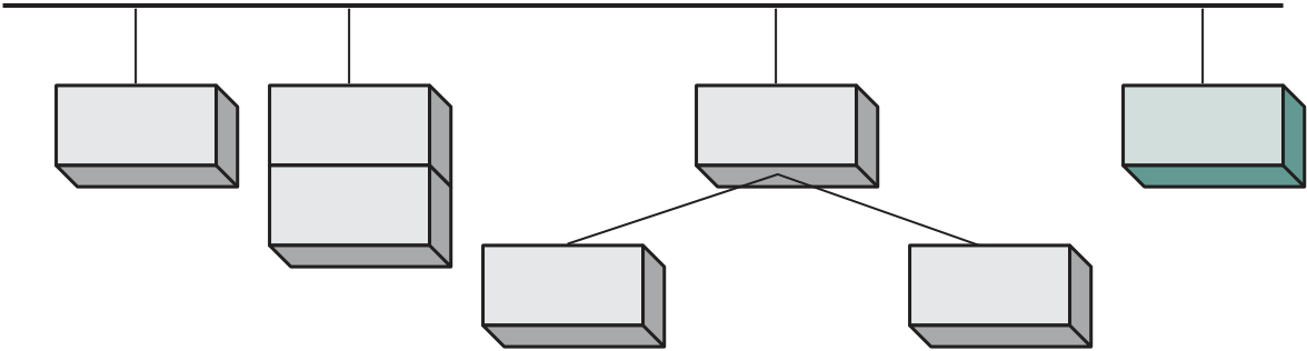
(a) Single-bus, detached DMA
| Processor |
|
DMA | Memory |
|---|
I/O bus
| I/O | I/O | I/O |
|---|
(c) I/O bus
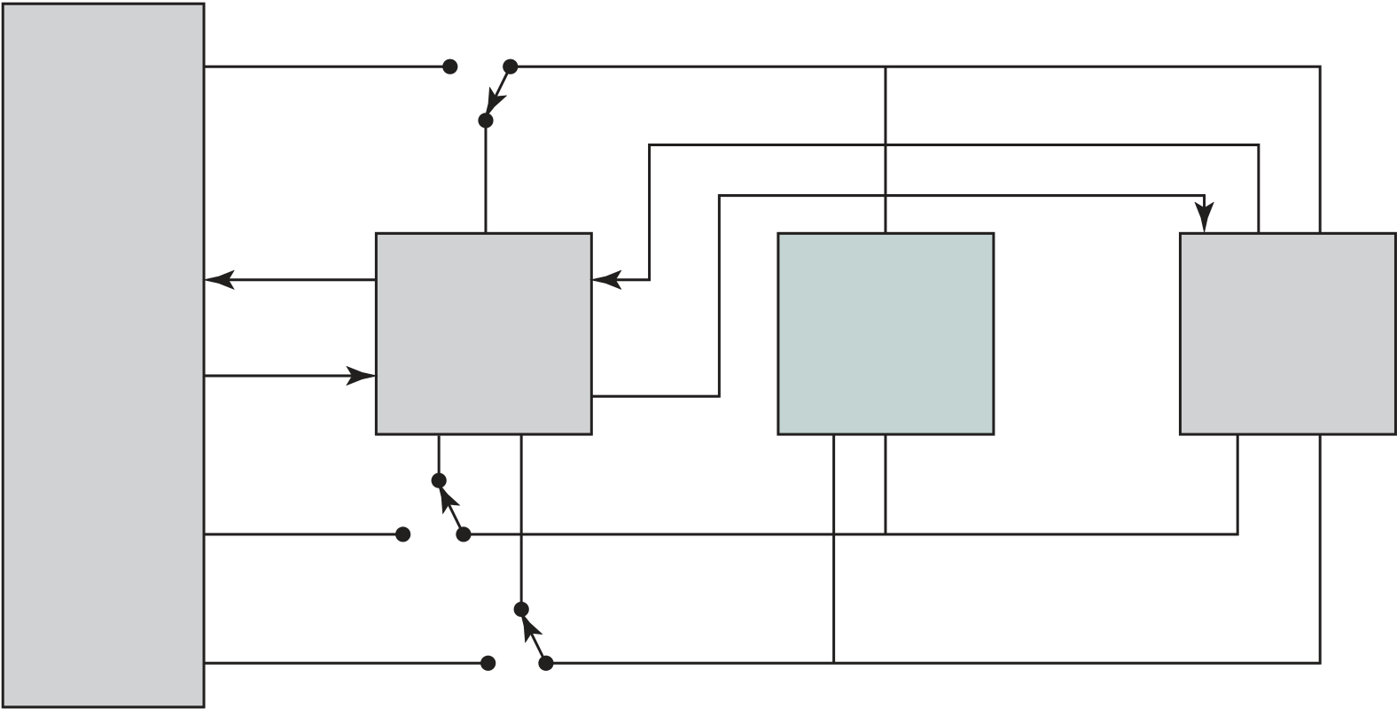
252 Chapter 7 / Input/Output
the DMA module can use the buses. For example, if the DMA module is to transfer a block of data from memory to disk, it will do the following:
1. The peripheral device (such as the disk controller) will request the service of DMA by pulling DREQ (DMA request) high.
6. After the DMA has finished its job it will deactivate HRQ, signaling the CPU that it can regain control over its buses.
7.5 / DIreCt MeMOry aCCess 253
■ Status: The processor reads this register to determine DMA status. Bits D0–D3 are used to indicate if channels 0–3 have reached their TC (terminal count). Bits D4–D7 are used by the processor to determine if any channel has a DMA request pending.
■ Mode: The processor sets this register to determine the mode of operation of the DMA. Bits D0 and D1 are used to select a channel. The other bits select various operation modes for the selected channel. Bits D2 and D3 determine if the transfer is from an I/O device to memory (write) or from memory to I/O (read), or a verify operation. If D4 is set, then the memory address regis-ter and the count register are reloaded with their original values at the end of a DMA data transfer. Bits D6 and D7 determine the way in which the 8237 is used. In single mode, a single byte of data is transferred. Block and demand modes are used for a block transfer, with the demand mode allowing for premature ending of the transfer. Cascade mode allows multiple 8237s to be cascaded to expand the number of channels to more than 4.
Table 7.2 Intel 8237A Registers
| Bit | Command | Status | Mode | Single Mask | All Mask |
|---|---|---|---|---|---|
|
Memory- to- memory E/D | Clear/set chan-nel 0 mask bit | |||
|
|
Clear/set chan-nel 1 mask bit | |||
| Clear/set mask bit | Clear/set chan-nel 2 mask bit | ||||
|
|
Clear/set chan-nel 3 mask bit | |||
| Channel 0 request |
|
|
|||
| Late/extended write selection | Channel 0 request | ||||
| Channel 0 request | |||||
|
|
Channel 0 request |
In this section, we will show how enabling the I/O function to have direct access to the cache can enhance performance, a technique known as direct cache access (DCA). Throughout this section, we are concerned only with the cache that is closest to main memory, referred to as the last- level cache. In some systems, this will be an L2 cache, in others an L3 cache.
To begin, we describe the way in which contemporary multicore systems use on- chip shared cache to enhance DMA performance. This approach involves ena-bling the DMA function to have direct access to the last- level cache. Next we exam-ine cache- related performance issues that manifest when high- speed network traffic is processed. From there, we look at several different strategies for DCA that are designed to enhance network protocol processing performance. Finally, this section describes a DCA approach implemented by Intel, referred to as Direct Data I/O.
The E5-2600/4600 can be configured with up to eight cores on a single chip. Each core has dedicated L1 and L2 caches. There is a shared L3 cache of up to 20 MB. The L3 cache is divided into slices, one associated with each core although each core can address the entire cache. Further, each slice has its own cache pipe-line, so that requests can be sent in parallel to the slices.
The bidirectional high- speed ring interconnect links cores, last- level cache, PCIe, and integrated memory controller (IMC).
The ring architecture provides good performance and scales well for multiple cores, up to a point. For systems with a greater number of cores, multiple rings are used, with each ring supporting some of the cores.
dmauseofthecache In traditional DMA operation, data are exchanged between main memory and an I/O device by means of the system interconnection structure, such as a bus, ring, or QPI point- to- point matrix. So, for example, if the Xeon E5-2600/4600 used a traditional DMA technique, output would proceed as follows. An I/O driver running on a core would send an I/O command to the I/O controller (labeled PCIe in Figure 7.16) with the location and size of the buffer in main memory containing the data to be transferred. The I/O controller issues a read request that is routed to the memory controller hub (MCH), which accesses the data on DDR3 memory and puts it on the system ring for delivery to the I/O controller. The L3 cache is not involved in this transaction and one or more off- chip memory reads are required. Similarly, for input, data arrive from the I/O controller and is delivered over the system ring to the MCH and written out to main memory. The MCH must also invalidate any L3 cache lines corresponding to the updated memory locations. In this case, one or more off- chip memory writes are required. Further, if an application wants to access the new data, a main memory read is required.
Chip boundary
To DDR3
memory
A final point. Although the output transfer is directly from cache to the I/O controller, the term direct cache access is not used for this feature. Rather, the term is reserved for the I/O protocol application, as described in the remainder of this section.
Cache- Related Performance Issues
1. Packet arrives: The NIC receives an incoming Ethernet packet. The NIC pro-cesses and strips off the Ethernet control information. This includes doing an error detection calculation. The remaining TCP/IP packet is then transferred to the system’s DMA module, which generally is part of the NIC. The NIC also creates a packet descriptor with information about the packet, such as its buffer location in memory.
258 Chapter 7 / Input/Output
6. Header is processed: The protocol software executes on the core to analyze the contents of the TCP and IP headers. This will likely include accessing a transport control block (TCB), which contains context information related to TCP. The TCB access may or may not trigger a cache miss, necessitating a main memory access.
7. Payload transferred: The data portion of the packet is transferred from the system buffer to the appropriate application buffer.
4. DMA transfer: The DMA module reads the packet descriptor, then a DMA transfer is performed from main memory or the last- level cache to the NIC. Note that DMA transfers invalidate the cache line in cache even in the case of a read (by the DMA module). If the line is modified, this causes a write back. The core does not do the invalidates. The invalidates happen when the DMA module reads the data.
5. NIC signals completion: After the transfer is complete, the NIC signals the driver on the core that originated the send signal.
Several strategies have been proposed for making more efficient use of caches for network I/O, with the general term direct cache access applied to all of these strategies.
The simplest strategy is one that was implemented as a prototype on a number of Intel Xeon processors between 2006 and 2010 [KUMA07, INTE08]. This form of DCA applies only to incoming network traffic. The DCA function in the mem-ory controller sends a prefetch hint to the core as soon as the data are available in system memory. This enables the core to prefetch the data packet from the system buffer, thus avoiding cache misses and the associated waste of core cycles.
packetinput First, we look at the case of a packet arriving at the NIC from the network. Figure 7.17a shows the steps involved for a DMA operation. The NIC initiates a memory write (1). Then the NIC invalidates the cache lines corresponding to the system buffer (2). Next, the DMA operation is performed, depositing the packet directly into main memory (3). Finally, after the appropriate core receives a DMA interrupt signal, the core can read the packet data from memory through the cache (4).
Before discussing the processing of an incoming packet using DDIO, we need to summarize the discussion of cache write policy from Chapter 4, and introduce a new technique. For the following discussion, there are issues relating to cache coher-ency that arise in a multiprocessor or multicore environment. These are discussed
| Core | Core |
|
|
||||||
|---|---|---|---|---|---|---|---|---|---|
| 1 | 1 |
|
|||||||
| Last–level cache | |||||||||
|
|||||||||
| 2 | |||||||||
| 1 | I/O | 4 | 1 | I/O | Main | ||||
| 3 | Core | memory | |||||||
| controller | |||||||||
|
|
||||||||
| Core | |||||||||
| 1 |
|
|
1 | ||||||
| Last–level cache | |||||||||
| 2 |
|
||||||||
| I/O | 1 |
|
|||||||
| 3 | |||||||||
| controller | |||||||||
| (c) Normal DMA transfer to I/O | |||||||||
Figure 7.17 Comparison of DMA and DDIO
in Chapter 17 but the details need not concern us here. Recall that there are two techniques for dealing with an update to a cache line:
■ Write allocate: The required line is loaded into the cache from main memory. Then, the line in the cache is updated by the write operation. This scheme is typically used with the write- back method.
■ Non- write allocate: The block is modified directly in main memory. No change is made to the cache. This scheme is typically used with the write- through method.
The DDIO strategy is effective for a network protocol application because the incoming data need not be retained for future use. The protocol application is going to write the data to an application buffer, and there is no need to temporarily store it in a system buffer.
Figure 7.17b shows the operation for DDIO input. The NIC initiates a memory write (1). Then the NIC invalidates the cache lines corresponding to the system buffer and deposits the incoming data in the cache (2). Finally, after the appropriate core receives a DCA interrupt signal, the core can read the packet data from the cache (3).
The Evolution of the I/O Function
As computer systems have evolved, there has been a pattern of increasing complex-ity and sophistication of individual components. Nowhere is this more evident than in the I/O function. We have already seen part of that evolution. The evolutionary steps can be summarized as follows:
4. The I/O module is given direct access to memory via DMA. It can now move a block of data to or from memory without involving the CPU, except at the beginning and end of the transfer.
5. The I/O module is enhanced to become a processor in its own right, with a specialized instruction set tailored for I/O. The CPU directs the I/O processor to execute an I/O program in memory. The I/O processor fetches and executes these instructions without CPU intervention. This allows the CPU to specify a sequence of I/O activities and to be interrupted only when the entire sequence has been performed.
Two types of I/O channels are common, as illustrated in Figure 7.18. A selector channel controls multiple high- speed devices and, at any one time, is dedicated to the transfer of data with one of those devices. Thus, the I/O chan-nel selects one device and effects the data transfer. Each device, or a small set of devices, is handled by a controller, or I/O module, that is much like the I/O mod-ules we have been discussing. Thus, the I/O channel serves in place of the CPU in controlling these I/O controllers. A multiplexor channel can handle I/O with multiple devices at the same time. For low- speed devices, a byte multiplexor accepts or transmits characters as fast as possible to multiple devices. For example, the resultant character stream from three devices with different rates and indi-vidual streams A1A2A3A4c ,B1B2B3B4c ,andC1C2C3C4c might be A1B1C1A2C2A3B2C3A4, and so on. For high- speed devices, a block multiplexor interleaves blocks of data from several devices.
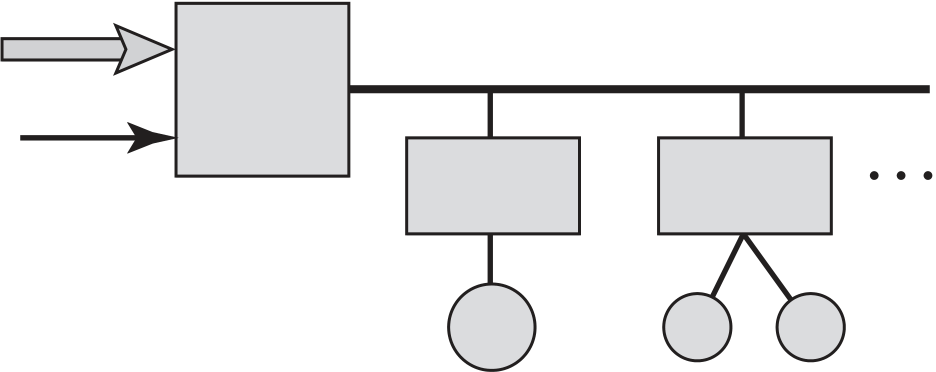
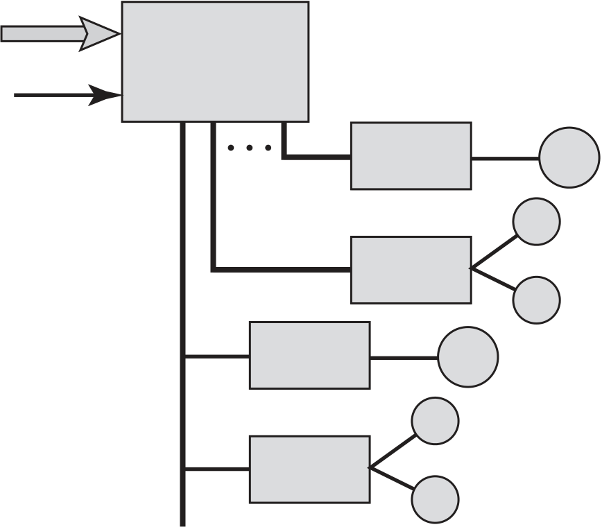
(a) Selector
Data and
address channel
to main memory
I/O
controllerI/O
controller
Universal Serial Bus (USB)
USB is widely used for peripheral connections. It is the default interface for slower- speed devices, such as keyboard and pointing devices, but is also commonly used for high- speed I/O, including printers, disk drives, and network adapters.
FireWire Serial Bus
FireWire was developed as an alternative to the small computer system interface (SCSI) to be used on smaller systems, such as personal computers, workstations, and servers. The objective was to meet the increasing demands for high I/O rates on these systems, while avoiding the bulky and expensive I/O channel technologies developed for mainframe and supercomputer systems. The result is the IEEE stan-dard 1394, for a High Performance Serial Bus, commonly known as FireWire.
SCSI is a once common standard for connecting peripheral devices (disks, modems, printers, etc.) to small and medium- sized computers. Although SCSI has evolved to higher data rates, it has lost popularity to such competitors as USB and FireWire in smaller systems. However, high- speed versions of SCSI remain popular for mass memory support on enterprise systems. For example, the IBM zEnterprise EC12 and other IBM mainframes offer support for SCSI, and a number of Seagate hard drive systems use SCSI.
The physical organization of SCSI is a shared bus, which can support up to 16 or 32 devices, depending on the generation of the standard. The bus provides for parallel transmission rather than serial, with a bus width of 16 bits on earlier gener-ations and 32 bits on later generations. Speeds range from 5 Mbps on the original SCSI- 1 specification to 160 Mbps on SCSI- 3 U3.
InfiniBand
InfiniBand is an I/O specification aimed at the high- end server market. The first version of the specification was released in early 2001 and has attracted numerous vendors. For example, IBM zEnterprise series of mainframes has relied heavily on InfiniBand for a number of years. The standard describes an architecture and speci-fications for data flow among processors and intelligent I/O devices. InfiniBand has become a popular interface for storage area networking and other large storage con-figurations. In essence, InfiniBand enables servers, remote storage, and other network devices to be attached in a central fabric of switches and links. The switch- based archi-tecture can connect up to 64,000 servers, storage systems, and networking devices. Infiniband is described in detail in Appendix J.
Ethernet
Ethernet is the predominant wired networking technology, used in homes, offices, data centers, enterprises, and wide- area networks. As Ethernet has evolved to sup-port data rates up to 100 Gbps and distances from a few meters to tens of km, it has become essential for supporting personal computers, workstations, servers, and massive data storage devices in organizations large and small.
■ 1995: 100 Mbps
■ 1998: 1 Gbps (gigabit per second, billion bits per second)
As the technology of antennas, wireless transmission techniques, and wireless protocol design has evolved, the IEEE 802.11 committee has been able to introduce standards for new versions of Wi- Fi at ever- higher speeds. Once the standard is issued, industry quickly develops the products. Here is a brief chronology, starting with the original standard, which was simply called IEEE 802.11, and showing the maximum data rate for each version:
■ 802.11 (1997): 2 Mbps (megabit per second, million bits per second)
■ 802.11ad (2012): 6.76 Gbps (billion bits per second)
■ 802.11ac (2014): 3.2 Gbps
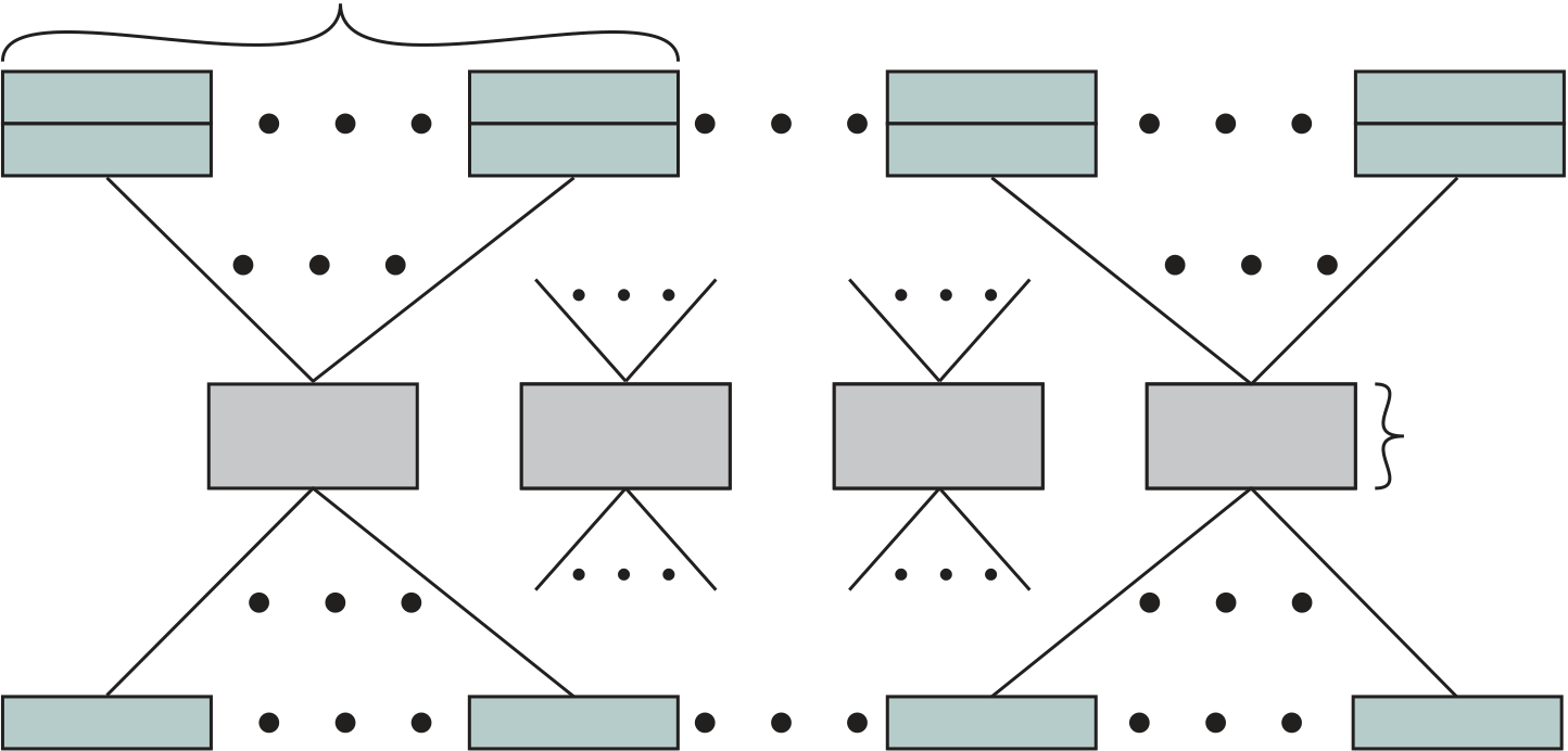
7.9 / IBM zenterprIse eC12 I/O struCture 267
| Channel | Subsystem | Subsystem | |||
|---|---|---|---|---|---|
| Channel |
|
≤ 256 channels per channel subsystem
■ Hardware system area (HSA): The HSA is a reserved part of the system mem-ory containing the I/O configuration. It is used by SAPs. A fixed amount of 32 GB is reserved, which is not part of the customer- purchased memory. This provides for greater configuration flexibility and higher availability by elimi-nating planned and preplanned outages.
■ Logical partitions: A logical partition is a form of virtual machine, which is in essence, a logical processor defined at the operating system level.3 Each CSS supports up to 16 logical partitions.
■ Channel: Channels are small processors that communicate with the I/O con-trol units (CUs). They manage the data transfer between memory and the external devices.
This elaborate structure enables the mainframe to manage a massive num-ber of I/O devices and communication links. All I/O processing is offloaded from the application and server processors, enhancing performance. The channel subsys-tem processors are somewhat general in configuration, enabling them to manage a wide variety of I/O duties and to keep up with evolving requirements. The chan-nel processors are specifically programmed for the I/O control units to which they interface.
■ Depth: 1.69 m (6.13 ft)
■ Height: 2.015 m (6.6 ft)
7.9 / IBM zenterprIse eC12 I/O struCture 269
cards
|
|---|
Figure 7.20 IBM zEC12 I/O Frames– Front View
270 Chapter 7 / Input/Output
| Book 1 | Book 3 | Book 4 | |||
|---|---|---|---|---|---|
| Memory | Memory | Memory | |||
| PU PU PU | PU PU PU | PU PU PU | |||
| SC1, SCO |
|
SC1, SCO | SC1, SCO | ||
| PU PU PU |
|
PU PU PU | PU PU PU | ||
| PCIe (8×) | HCA2 (8×) | HCA2 (8×) | |||
| PCIe | PCIe | PCIe | InfniB and | ||
| switch | switch | switch | multiplexor | ||
| Channels | Ports | ||||
Fibre Channel 10-Gbps ESCON 1-Gbps controller Ethernet controller Ethernet controller
PCIe I/O Drawer I/O Cage & I/O Drawer
Key Terms
7.7 |
|
|---|
7.9 7.10 7.15 |
|
|---|
7.10 / Key terMs, revIew QuestIOns, anD prOBleMs 273
b. What would be the maximum attainable data transfer rate?
7.21 |
|
|---|
274 Chapter 7 / Input/Output
b. Now assume that there is no alarm clock. Instead Apple- eater has a flag that she can wave whenever she needs an apple. Suggest a new solution. Would it be help-ful for Apple- server also to have a flag? If so, incorporate this into the solution. Discuss the drawbacks of this approach.
Operating SyStem SuppOrt
8.1 Operating System Overview
Operating System Objectives and Functions Types of Operating Systems8.6 Key Terms, Review Questions, and Problems
275
|
|---|
Operating System Objectives and Functions
An OS is a program that controls the execution of application programs and acts as an interface between applications and the computer hardware. It can be thought of as having two objectives:
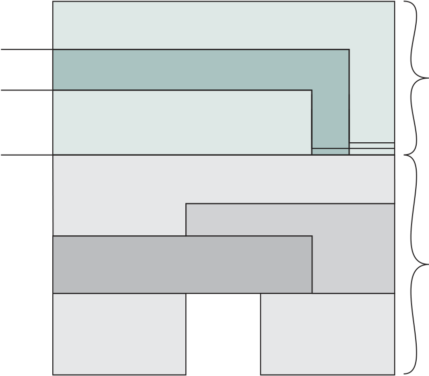
8.1 / Operating SyStem Overview 277
Execution hardware
| System interconnect | Memory | Hardware |
|---|---|---|
| translation | ||
| (bus) | ||
| I/O devices |
|
|
| and | ||
| networking |
■ Program creation: The OS provides a variety of facilities and services, such as editors and debuggers, to assist the programmer in creating programs. Typi-cally, these services are in the form of utility programs that are not actually part of the OS but are accessible through the OS.
■ Program execution: A number of steps need to be performed to execute a program. Instructions and data must be loaded into main memory, I/O devices and files must be initialized, and other resources must be prepared. The OS handles all of this for the user.
■ Error detection and response: A variety of errors can occur while a computer system is running. These include internal and external hardware errors, such as a memory error, or a device failure or malfunction; and various software errors, such as arithmetic overflow, attempt to access forbidden memory loca-tion, and inability of the OS to grant the request of an application. In each case, the OS must make the response that clears the error condition with the least impact on running applications. The response may range from ending the program that caused the error, to retrying the operation, to simply reporting the error to the application.
■ Accounting: A good OS collects usage statistics for various resources and monitors performance parameters such as response time. On any system, this information is useful in anticipating the need for future enhancements and in tuning the system to improve performance. On a multiuser system, the infor-mation can be used for billing purposes. Figure 8.1 also indicates three key interfaces in a typical computer system:
Can we say that the OS controls the movement, storage, and processing of data? From one point of view, the answer is yes: By managing the computer’s resources, the OS is in control of the computer’s basic functions. But this control is exercised in a curious way. Normally, we think of a control mechanism as something external to that which is controlled, or at least as something that is a distinct and separate part of that which is controlled. (For example, a residential heating system
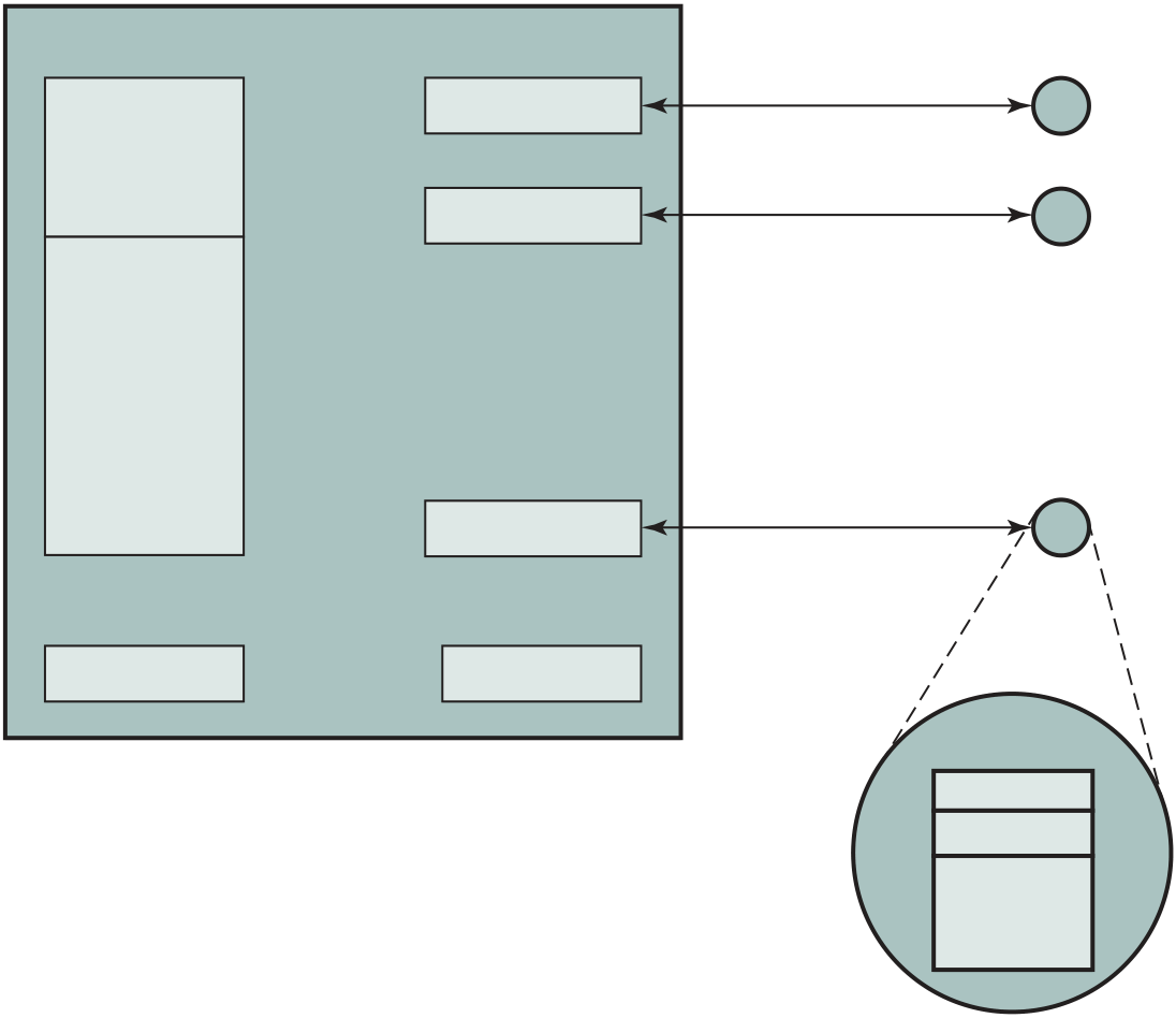
Like other computer programs, the OS provides instructions for the proces-sor. The key difference is in the intent of the program. The OS directs the processor in the use of the other system resources and in the timing of its execution of other programs. But in order for the processor to do any of these things, it must cease executing the OS program and execute other programs. Thus, the OS relinquishes control for the processor to do some “useful” work and then resumes control long enough to prepare the processor to do the next piece of work. The mechanisms involved in all this should become clear as the chapter proceeds.
Figure 8.2 suggests the main resources that are managed by the OS. A portion of the OS is in main memory. This includes the kernel, or nucleus, which contains the most frequently used functions in the OS and, at a given time, other portions of the OS currently in use. The remainder of main memory contains user programs and data. The allocation of this resource (main memory) is controlled jointly by the OS and memory- management hardware in the processor, as we will see. The OS decides when an I/O device can be used by a program in execution, and controls access to and
| Processor | • • • |
|
|---|
Storage
use of files. The processor itself is a resource, and the OS must determine how much processor time is to be devoted to the execution of a particular user program. In the case of a multiple- processor system, this decision must span all of the processors.
Types of Operating Systems
■ Scheduling: Most installations used a sign- up sheet to reserve processor time. Typically, a user could sign up for a block of time in multiples of a half hour or so. A user might sign up for an hour and finish in 45 minutes; this would result in wasted computer idle time. On the other hand, the user might run into problems, not finish in the allotted time, and be forced to stop before resolving the problem.
■ Setup time: A single program, called a job, could involve loading the com-piler plus the high- level language program (source program) into memory, saving the compiled program (object program), and then loading and linking together the object program and common functions. Each of these steps could involve mounting or dismounting tapes, or setting up card decks. If an error occurred, the hapless user typically had to go back to the beginning of the setup sequence. Thus a considerable amount of time was spent just in setting up the program to run.
To improve utilization, simple batch operating systems were developed. With such a system, also called a monitor, the user no longer has direct access to the pro-cessor. Rather, the user submits the job on cards or tape to a computer operator, who batches the jobs together sequentially and places the entire batch on an input device, for use by the monitor.
To understand how this scheme works, let us look at it from two points of view: that of the monitor and that of the processor. From the point of view of the monitor, the monitor controls the sequence of events. For this to be so, much of the monitor must always be in main memory and available for execution (Figure 8.3). That portion is referred to as the resident monitor. The rest of the monitor consists of utilities and common functions that are loaded as subroutines to the user pro-gram at the beginning of any job that requires them. The monitor reads in jobs one at a time from the input device (typically a card reader or magnetic tape drive). As it is read in, the current job is placed in the user program area, and control is passed to this job. When the job is completed, it returns control to the monitor, which imme-diately reads in the next job. The results of each job are printed out for delivery to the user.
Now consider this sequence from the point of view of the processor. At a certain point in time, the processor is executing instructions from the portion of main mem-ory containing the monitor. These instructions cause the next job to be read in to another portion of main memory. Once a job has been read in, the processor will encounter in the monitor a branch instruction that instructs the processor to con-tinue execution at the start of the user program. The processor will then execute the instruction in the user’s program until it encounters an ending or error condi-tion. Either event causes the processor to fetch its next instruction from the monitor program. Thus the phrase “control is passed to a job” simply means that the pro-cessor is now fetching and executing instructions in a user program, and “control is returned to the monitor” means that the processor is now fetching and executing instructions from the monitor program.
It should be clear that the monitor handles the scheduling problem. A batch of jobs is queued up, and jobs are executed as rapidly as possible, with no intervening idle time.
8.1 / Operating SyStem Overview 283
■ Interrupts: Early computer models did not have this capability. This feature gives the OS more flexibility in relinquishing control to and regaining control from user programs.
Processor time alternates between execution of user programs and execution of the monitor. There have been two sacrifices: Some main memory is now given over to the monitor and some processor time is consumed by the monitor. Both of these are forms of overhead. Even with this overhead, the simple batch system improves utilization of the computer.
= 0.032 = 3.2%
Figure 8.4 System Utilization Example
| Program A | ||
|---|---|---|
| Time | ||
Program B Combined |
|
||||||
|---|---|---|---|---|---|---|---|
| Time | |||||||
This inefficiency is not necessary. We know that there must be enough memory to hold the OS (resident monitor) and one user program. Suppose that there is room for the OS and two user programs. Now, when one job needs to wait for I/O, the pro-cessor can switch to the other job, which likely is not waiting for I/O (Figure 8.5b). Furthermore, we might expand memory to hold three, four, or more programs and switch among all of them (Figure 8.5c). This technique is known as multiprogram-ming, or multitasking.1 It is the central theme of modern operating systems.
1The term multitasking is sometimes reserved to mean multiple tasks within the same program that may be handled concurrently by the OS, in contrast to multiprogramming, which would refer to multiple processes from multiple programs. However, it is more common to equate the terms multitasking and multiprogramming, as is done in most standards dictionaries (e.g., IEEE Std 100-1992, The New IEEE Standard Dictionary of Electrical and Electronics Terms).
Figure 8.6 Utilization Histograms
and DMA. With interrupt- driven I/O or DMA, the processor can issue an I/O com-mand for one job and proceed with the execution of another job while the I/O is car-ried out by the device controller. When the I/O operation is complete, the processor is interrupted and control is passed to an interrupt- handling program in the OS. The OS will then pass control to another job.
8.2 / SCheduling 287
Table 8.3 Batch Multiprogramming versus Time Sharing
|
||
|
8.2 Scheduling
The key to multiprogramming is scheduling. In fact, four types of scheduling are typically involved (Table 8.4). We will explore these presently. But first, we introduce the concept of process. This term was first used by the designers of the Multics OS in the 1960s. It is a somewhat more general term than job. Many definitions have been given for the term process, including
Long- Term Scheduling
The long- term scheduler determines which programs are admitted to the system for processing. Thus, it controls the degree of multiprogramming (number of processes in memory). Once admitted, a job or user program becomes a process and is added to the queue for the short- term scheduler. In some systems, a newly created pro-cess begins in a swapped- out condition, in which case it is added to a queue for the medium- term scheduler.
In a batch system, or for the batch portion of a general- purpose OS, newly submit-ted jobs are routed to disk and held in a batch queue. The long- term scheduler creates processes from the queue when it can. There are two decisions involved here. First, the scheduler must decide that the OS can take on one or more additional processes. Second, the scheduler must decide which job or jobs to accept and turn into processes. The criteria used may include priority, expected execution time, and I/O requirements.
For interactive programs in a time- sharing system, a process request is gen-erated when a user attempts to connect to the system. Time- sharing users are not simply queued up and kept waiting until the system can accept them. Rather, the OS will accept all authorized comers until the system is saturated, using some pre-defined measure of saturation. At that point, a connection request is met with a message indicating that the system is full and the user should try again later.
processstates To understand the operation of the short- term scheduler, we need to consider the concept of a process state. During the lifetime of a process, its status will change a number of times. Its status at any point in time is referred to as a state. The term state is used because it connotes that certain information exists that defines the status at that point. At minimum, there are five defined states for a process (Figure 8.7):
■ New: A program is admitted by the high- level scheduler but is not yet ready to execute. The OS will initialize the process, moving it to the ready state.
| New | Admit | Ready | Dispatch | Running | Exit |
|---|
Blocked
Figure 8.7 Five- State Process Model
■ Halted: The process has terminated and will be destroyed by the OS.
For each process in the system, the OS must maintain information indicat-ing the state of the process and other information necessary for process execution. For this purpose, each process is represented in the OS by a process control block (Figure 8.8), which typically contains:
■ Memory pointers: The starting and ending locations of the process in memory.
■ Context data: These are data that are present in registers in the processor while the process is executing, and they will be discussed in Part Three. For now, it is enough to say that these data represent the “context” of the process. The context data plus the program counter are saved when the process leaves the running state. They are retrieved by the processor when it resumes execu-tion of the process.
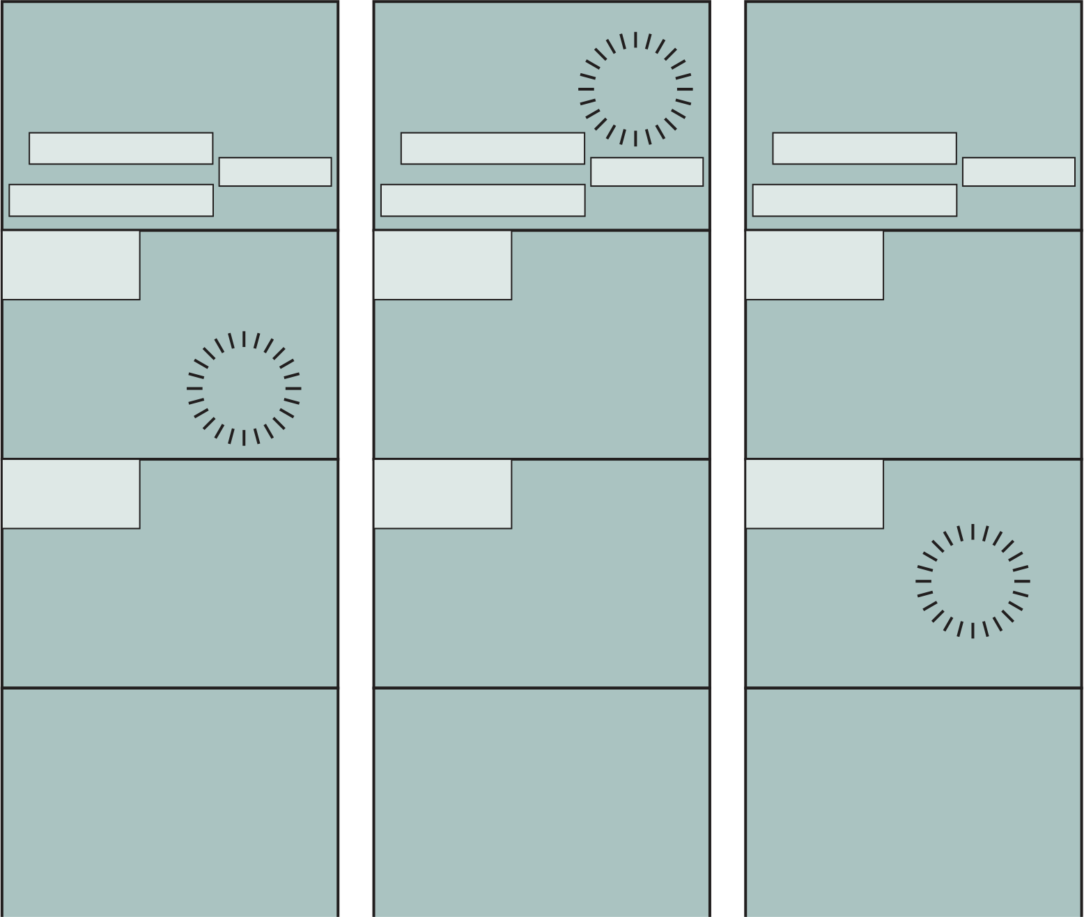
290 Chapter 8 / Operating SyStem SuppOrt
|
Operating system | Operating system |
|---|
In
control
|
B | B |
|---|---|---|
|
"Ready" | "Running" |
8.2 / SCheduling 291
We begin at a point in time when process A is running. The processor is exe-cuting instructions from the program contained in A’s memory partition. At some later point in time, the processor ceases to execute instructions in A and begins exe-cuting instructions in the OS area. This will happen for one of three reasons:
This simple example highlights the basic functioning of the short- term sched-uler. Figure 8.10 shows the major elements of the OS involved in the multiprogram-ming and scheduling of processes. The OS receives control of the processor at the
Operating system
| Service call | Service | Long- | Short- | |
|---|---|---|---|---|
| call | ||||
| from process | ||||
| Interrupt | ||||
| Interrupt | term | term | ||
| from process | ||||
| queue | ||||
| Interrupt |
|
|||
| from I/O |
|
|||
292 Chapter 8 / Operating SyStem SuppOrt
Figure 8.11 Queuing Diagram Representation of Processor Scheduling
8.3 / memOry management 293
Effective memory management is vital in a multiprogramming system. If only a few processes are in memory, then for much of the time all of the processes will be waiting for I/O and the processor will be idle. Thus, memory needs to be allocated efficiently to pack as many processes into memory as possible.
Swapping
294 Chapter 8 / Operating SyStem SuppOrt
| Disk storage |
|---|
(a) Simple job scheduling
Disk storage
| Intermediate | Main | |
|---|---|---|
| memory | ||
| queue | Operating | |
| Long-term | system | |
| queue |
kicked out of memory. The OS then brings in another process from the intermedi-ate queue, or it honors a new process request from the long- term queue. Execution then continues with the newly arrived process.
Swapping, however, is an I/O operation, and therefore there is the potential for making the problem worse, not better. But because disk I/O is generally the fastest I/O on a system (e.g., compared with tape or printer I/O), swapping will usu-ally enhance performance. A more sophisticated scheme, involving virtual memory, improves performance over simple swapping. This will be discussed shortly. But first, we must prepare the ground by explaining partitioning and paging.
(a) Equal-size partitions
A more efficient approach is to use variable- size partitions. When a process is brought into memory, it is allocated exactly as much memory as it requires and no more.

■ Addresses of instructions, used for branching instructions
| Operating |
|
20M | |||||
|---|---|---|---|---|---|---|---|
| system | system | ||||||
| Process 1 | |||||||
|
Process 2 | 14M | |||||
|
|||||||
| Process 3 | 18M | ||||||
| 4M | |||||||
| (a) | (b) | 20M | (c) | (d) | 14M | ||
| Operating | Operating | Operating | |||||
| system | system | system | system | ||||
| Process 2 | |||||||
| Process 1 | Process 1 |
6M
Paging
Both unequal fixed- size and variable- size partitions are inefficient in the use of mem-ory. Suppose, however, that memory is partitioned into equal fixed- size chunks that are relatively small, and that each process is also divided into small fixed- size chunks of some size. Then the chunks of a program, known as pages, could be assigned to available chunks of memory, known as frames, or page frames. At most, then, the wasted space in memory for that process is a fraction of the last page.
| Process A | 13 | Process A | 13 | |||||||
|---|---|---|---|---|---|---|---|---|---|---|
|
||||||||||
|
||||||||||
| Page 0 | 14 | Page 0 | 14 |
|
||||||
| Page 1 | Page 1 | |||||||||
| Page 2 | Page 2 |
|
||||||||
| Page 3 | 15 | Page 3 | 15 | |||||||
| Free frame list | 16 | Free frame list | 16 | |||||||
|
||||||||||
| 13 | 17 | 20 | 17 | |||||||
| 14 |
|
|||||||||
| 15 | 18 | Process A | 18 | |||||||
| 18 | page table | |||||||||
| 20 | ||||||||||
| 19 | 19 | |||||||||
| 20 | 20 | |||||||||
| (a) Before | ||||||||||
| (b) After |
Figure 8.15 Allocation of Free Frames
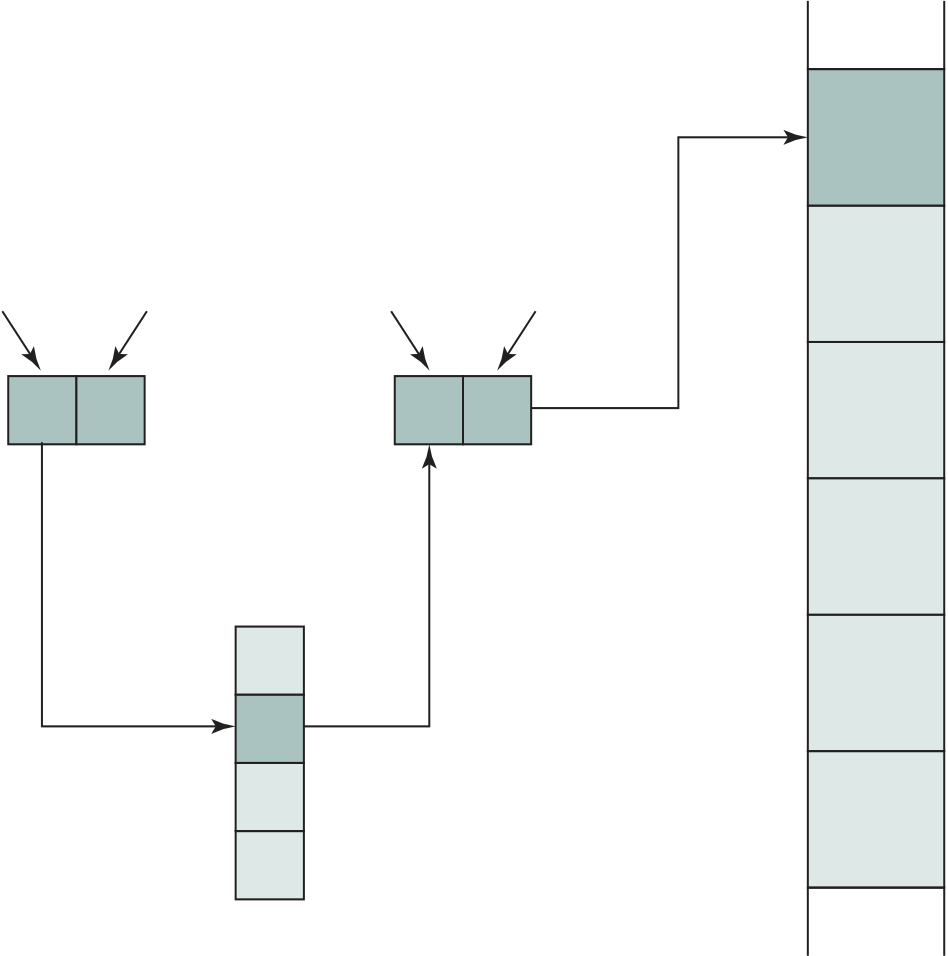
Main
memory
16
| 18 | 17 |
|---|
13
Virtual Memory
demandpaging With the use of paging, truly effective multiprogramming systems came into being. Furthermore, the simple tactic of breaking a process up into pages led to the development of another important concept: virtual memory.
Page Replacement Algorithm Simulators
A discussion of page replacement algorithms is beyond the scope of this chap-ter. A potentially effective technique is least recently used (LRU), the same algo-rithm discussed in Chapter 4 for cache replacement. In practice, LRU is difficult to implement for a virtual memory paging scheme. Several alternative approaches that seek to approximate the performance of LRU are in use; see Appendix K for details.
pagetablestructure The basic mechanism for reading a word from memory involves the translation of a virtual, or logical, address, consisting of page number and offset, into a physical address, consisting of frame number and offset, using a page table. Because the page table is of variable length, depending on the size of the process, we cannot expect to hold it in registers. Instead, it must be in main memory to be accessed. Figure 8.16 suggests a hardware implementation of this scheme. When a particular process is running, a register holds the starting address of the page table for that process. The page number of a virtual address is used to index that table and look up the corresponding frame number. This is combined with the offset portion of the virtual address to produce the desired real address.
In most systems, there is one page table per process. But each process can occupy huge amounts of virtual memory. For example, in the VAX architecture, each pro-cess can have up to 231= 2 Gbytes of virtual memory. Using 29= 512 - byte pages, that means that as many as 222 page table entries are required per process. Clearly, the amount of memory devoted to page tables alone could be unacceptably high. To overcome this problem, most virtual memory schemes store page tables in virtual memory rather than real memory. This means that page tables are subject to paging just as other pages are. When a process is running, at least a part of its page table must be in main memory, including the page table entry of the currently executing page. Some processors make use of a two- level scheme to organize large page tables. In this scheme, there is a page directory, in which each entry points to a page table. Thus, if the length of the page directory is X, and if the maximum length of a page table is Y, then a process can consist of up to X * Y pages. Typically, the maximum length of a page table is restricted to be equal to one page. We will see an example of this two- level approach when we consider the Intel x86 later in this chapter.
8.3 / memOry management 301
Virtual address
| Page # | Page # | Control | ||||
|---|---|---|---|---|---|---|
| bits | ||||||
| Hash | m bits |
|
||||
| ID | Chain | |||||
|
||||||
Figure 8.17 Inverted Page Table Structure
inverted page table for each real memory page frame rather than one per virtual page. Thus a fixed proportion of real memory is required for the tables regardless of the number of processes or virtual pages supported. Because more than one virtual address may map into the same hash table entry, a chaining technique is used for managing the overflow. The hashing technique results in chains that are typically short— between one and two entries. The page table’s structure is called inverted because it indexes page table entries by frame number rather than by virtual page number.
Start
| Return to | CPU checks the TLB |
|
|---|---|---|
| faulted instruction | ||
| Page table | ||
| entry in | ||
| TLB? |
Yes
| CPU activates |
|
Update TLB |
|---|---|---|
| I/O hardware | ||
| Page transferred | CPU generates | |
| from disk to | ||
| main memory | ||
| physical address | ||
| Memory | ||
| full? | ||
| No | ||
Note that the virtual memory mechanism must interact with the cache system (not the TLB cache, but the main memory cache). This is illustrated in Figure 8.19. A virtual address will generally be in the form of a page number, offset. First, the memory system consults the TLB to see if the matching page table entry is present. If it is, the real (physical) address is generated by combining the frame number with the offset. If not, the entry is accessed from a page table. Once the real address is generated, which is in the form of a tag and a remainder, the cache is consulted to see if the block containing that word is present (see Figure 4.5). If so, it is returned to the processor. If not, the word is retrieved from main memory.
The reader should be able to appreciate the complexity of the processor hard-ware involved in a single memory reference. The virtual address is translated into a real address. This involves reference to a page table, which may be in the TLB, in
| Cache operation |
|---|
Main
memoryPage table
There is another way in which addressable memory can be subdivided, known as segmentation. Whereas paging is invisible to the programmer and serves the purpose of providing the programmer with a larger address space, segmentation is usually visible to the programmer and is provided as a convenience for organizing programs and data and as a means for associating privilege and protection attributes with instructions and data.
Segmentation allows the programmer to view memory as consisting of multiple address spaces or segments. Segments are of variable, indeed dynamic, size. Typi-cally, the programmer or the OS will assign programs and data to different segments. There may be a number of program segments for various types of programs as well as a number of data segments. Each segment may be assigned access and usage rights. Memory references consist of a (segment number, offset) form of address.
3. It lends itself to sharing among processes. A programmer can place a utility program or a useful table of data in a segment that can be addressed by other processes.
4. It lends itself to protection. Because a segment can be constructed to contain a well- defined set of programs or data, the programmer or a system administra-tor can assign access privileges in a convenient fashion.
The x86 includes hardware for both segmentation and paging. Both mechanisms can be disabled, allowing the user to choose from four distinct views of memory:
■ Unsegmented unpaged memory: In this case, the virtual address is the same as the physical address. This is useful, for example, in low- complexity, high- performance controller applications.
Segmentation
When segmentation is used, each virtual address (called a logical address in the x86 documentation) consists of a 16-bit segment reference and a 32-bit offset. Two bits of the segment reference deal with the protection mechanism, leaving 14 bits for specifying a particular segment. Thus, with unsegmented memory, the user’s virtual memory is 232= 4 Gbytes. With segmented memory, the total virtual memory space as seen by a user is 246= 64 terabytes (Tbytes). The physical address space employs a 32-bit address for a maximum of 4 Gbytes.
The access attribute of a data segment specifies whether read/write or read- only accesses are permitted. For program segments, the access attribute specifies read/execute or read- only access.
The address translation mechanism for segmentation involves mapping a vir-tual address into what is referred to as a linear address (Figure 8.20b). A virtual address consists of the 32-bit offset and a 16-bit segment selector (Figure 8.20a). An instruction fetching or storing an operand specifies the offset and a register contain-ing the segment selector. The segment selector consists of the following fields:
RPL = Requestor privilege level
(a) Segment selector
| 31 | 22 21 | 12 11 | 0 |
|---|
(b) Linear address
| 31 | 24 | 23 | 22 | 20 | 16 | 15 | 14 | 13 | 12 | 8 | 0 |
|---|
|
L |
|
|
|---|---|---|---|
| P | |||
| G | S |
|
|
(c) Segment descriptor (segment table entry)
| Page frame address 31...12 | AVL | P S | 0 | A | P W T |
U S | R W |
P |
|---|
|
|||||
|---|---|---|---|---|---|
| P |
|
US = User/supervisor | |||
| A | |||||
| P | |||||
(d) Page directory entry
| Page frame address 31...12 | AVL | D | A | P W T |
U S | R W |
P |
|---|
■ Segment Number: The number of the segment. This serves as an index into the segment table.
■ Requested Privilege Level (RPL): The privilege level requested for this access.
|
|---|
Segmentation is an optional feature and may be disabled. When segmentation is in use, addresses used in programs are virtual addresses and are converted into linear addresses, as just described. When segmentation is not in use, linear addresses are used in programs. In either case, the following step is to convert that linear address into a real 32-bit address.
To understand the structure of the linear address, you need to know that the x86 paging mechanism is actually a two- level table lookup operation. The first level is a page directory, which contains up to 1024 entries. This splits the 4-Gbyte linear memory space into 1024 page groups, each with its own page table, and each 4 Mbytes in length. Each page table contains up to 1024 entries; each entry corresponds to a single 4-Kbyte page. Memory management has the option of using one page directory for all processes, one page directory for each process, or some combination of the two. The page directory for the current task is always in main memory. Page tables may be in virtual memory.
| Segment | Segment | Page directory |
|
Page |
|---|---|---|---|---|
| descriptor | Lin. Addr. | Entry | ||
| Phy. Addr. |
Entry
8.5 / arm memOry management 309
Finally, the x86 includes a new extension not found on the earlier 80386 or 80486, the provision for two page sizes. If the PSE (page size extension) bit in con-trol register 4 is set to 1, then the paging unit permits the OS programmer to define a page as either 4 Kbyte or 4 Mbyte in size.
Memory System Organization
Figure 8.22 provides an overview of the memory management hardware in the ARM for virtual memory. The virtual memory translation hardware uses one or two levels of tables for translation from virtual to physical addresses, as explained subsequently. The translation lookaside buffer (TLB) is a cache of recent page table entries. If an entry is available in the TLB, then the TLB directly sends a physical address to main memory for a read or write operation. As explained in Chapter 4, data is exchanged
| Access | TLB | Virtual | Physical | Main | ||
|---|---|---|---|---|---|---|
| Virtual address | address | |||||
| control | ||||||
|
|
|||||
| hardware | ||||||
| Abort | ||||||
| Physical address | ||||||
| ARM | Control | Cache | memory | |||
| bits | ||||||
| core | ||||||
| and | Cache | |||||
| write | line fetch | |||||
| buffer | hardware | |||||
Figure 8.22 ARM Memory System Overview
310 Chapter 8 / Operating SyStem SuppOrt
■ Supersections (optional): Consist of 16-MB blocks of main memory.
■ Sections: Consist of 1-MB blocks of main memory.
■ Level 2 table: Holds level 2 descriptors that contain the base address and trans-lation properties for a Small page or a Large page. A level 2 table requires 1 kB of memory.
The memory- management unit (MMU) translates virtual addresses generated by the processor into physical addresses to access main memory, and also derives and checks the access permission. Translations occur as the result of a TLB miss, and start with a first- level fetch. A section- mapped access only requires a first- level fetch, whereas a page- mapped access also requires a second- level fetch.
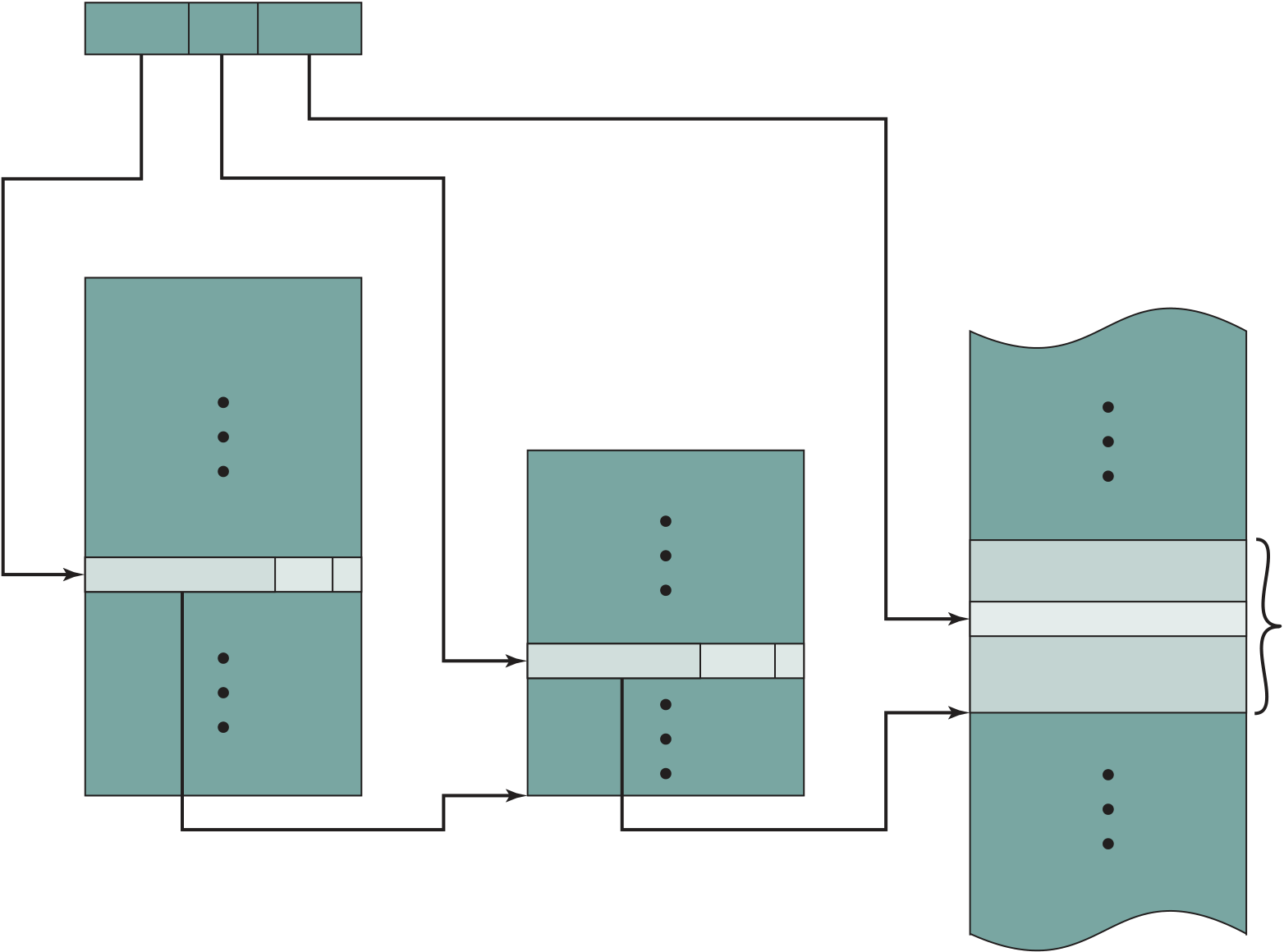
8.5 / arm memOry management 311
| 0 | 01 | 0 |
|
|
Small page (4 kB) |
|---|
■ Bits [1:0] = 01: and bit 19 = 0: The entry is a section descriptor for its asso- ciated virtual addresses.
■ Bits [1:0] = 01: and bit 19 = 1: The entry is a supersection descriptor for its associated virtual addresses.
312 Chapter 8 / Operating SyStem SuppOrt
| Fault | 31 | 24 23 |
|
14 | 12 | 11 | 10 | 9 | 5 | 4 | 3 | 2 | 1 | 0 | |||
|---|---|---|---|---|---|---|---|---|---|---|---|---|---|---|---|---|---|
| IGN | 0 | 0 | |||||||||||||||
| Page table | Coarse page table base address | ||||||||||||||||
| Section | |||||||||||||||||
| Supersection |
|
||||||||||||||||
| [35:32] | |||||||||||||||||
|
24 | 20 | 0 | |||||||
|---|---|---|---|---|---|---|---|---|---|---|
|
20 |
|
0 | |||||||
| 20 | 12 | 0 | ||||||||
| 20 | 16 | 12 | 0 | |||||||
(c) Virtual memory address formats
Access Control
The AP access control bits in each table entry control access to a region of memory by a given process. A region of memory can be designated as no access, read only, or read- write. Further, the region can be designated as privileged access only, reserved for use by the OS and not by applications.
■ Clients: Users of domains (execute programs and access data) that must observe the access permissions of the individual sections and/or pages that make up that domain.
■ Managers: Control the behavior of the domain (the current sections and pages in the domain, and the domain access), and bypass the access permissions for table entries in that domain.
|
|
|---|
8.6 / Key termS, review QueStiOnS, and prOblemS 315
8.8 Must the pages of a process in main memory be contiguous?
8.2 8.3 |
|||
|---|---|---|---|
| ■ | |||
| ■ | |||
| ■ | Processor utilization = percentage of time that the processor is active (not waiting). | ||
|
|||
page frames. Is there any difference in the page fault rate if A were stored in virtual
memory by rows or columns? Explain.
| Valid bit | Reference bit | Modify bit | ||
|---|---|---|---|---|
| 0 | 1 | 1 | 0 | 4 |
| 1 | 1 | 1 | 1 | 7 |
| 2 | 0 | 0 | 0 | — |
| 3 | 1 | 0 | 0 | 2 |
| 4 | 0 | 0 | 0 | — |
| 5 | 1 | 0 | 1 | 0 |
b. What physical address, if any, would each of the following virtual addresses corre- spond to? (Do not try to handle any page faults, if any.)
i. 1052
ii. 2221
iii. 5499
| 8.9 |
|---|
Assume that a least recently used page replacement policy is adopted. Plot a graph of page hit ratio (fraction of page references in which the page is in main memory) as a function of main- memory page capacity n for 1 … n … 8. Assume that main memory is initially empty.
a[i] = b[i] + c[i];
is executed in a memory with page size of 1000 words. Let n = 1000. Using a machine that has a full range of register- to- register instructions and employs index registers, write a hypothetical program to implement the foregoing statement. Then show the sequence of page references during execution.
|
|---|
b. What is the maximum logical address space for the task?
c. Assume that an element in physical location 00021ABC is accessed by this task.
And Logic
CHAPTER
9.4 Converting Between Binary and Decimal
Integers
9.1 / The Decimal SySTem 319
|
|---|
9.1 THE DECIMAL SYSTEM
In everyday life we use a system based on decimal digits (0, 1, 2, 3, 4, 5, 6, 7, 8, 9) to represent numbers, and refer to the system as the decimal system. Consider what the number 83 means. It means eight tens plus three:
83 = (8 * 101) + (3 * 100)
4728 = (4 * 103) + (7 * 102) + (2 * 101) + (8 * 100)The same principle holds for decimal fractions, but negative powers of 10 are used. Thus, the decimal fraction 0.256 stands for 2 tenths plus 5 hundredths plus 6 thousandths:
In any number, the leftmost digit is referred to as the most significant digit, because it carries the highest value. The rightmost digit is called the least significant digit. In the preceding decimal number, the 4 on the left is the most significant digit and the 6 on the right is the least significant digit.
Table 9.1 shows the relationship between each digit position and the value assigned to that position. Each position is weighted 10 times the value of the position to the right and one-tenth the value of the position to the left. Thus, positions rep-resent successive powers of 10. If we number the positions as indicated in Table 9.1, then position i is weighted by the value 10i.
One other observation is worth making. Consider the number 509 and ask how many tens are in the number. Because there is a 0 in the tens position, you might be tempted to say there are no tens. But there are in fact 50 tens. What the 0 in the tens position means is that there are no tens left over that cannot be lumped into the hundreds, or thousands, and so on. Therefore, because each position holds only the leftover numbers that cannot be lumped into higher positions, each digit position needs to have a value of no greater than nine. Nine is the maximum value that a position can hold before it flips over into the next higher position.
9.2 POSITIONAL NUMBER SYSTEMS
The decimal system, then, is a special case of a positional number system with radix 10 and with digits in the range 0 through 9.
| 4 | 3 | 2 | 1 | 0 | -1 | |
|---|---|---|---|---|---|---|
| 74 | 73 | 72 | 71 | 70 | 7-1 | |
|
2401 | 343 | 49 | 7 | 1 | 1/7 |
9.4 / coNveRTiNg beTweeN biNaRy aND Decimal 321
12 = 110
To represent larger numbers, as with decimal notation, each digit in a binary num-ber has a value depending on its position:
In general, for the binary representation of Y = 5cb2b1b0.b-1b-2b-3c6, the Y = a (bi * 2i) (9.3) i
9.4 CONVERTING BETWEEN BINARY AND DECIMAL
bm-1bm-2 cb2b1b0bi = 0or1
has the value
N1 = 2 * N2 + R1R1 = 0or1 so that
N = 2(2N2 + R1) + R0 = (N2 * 22) + (R1 * 21) + R0 If next
For the fractional part, recall that in binary notation, a number with a value between 0 and 1 is represented by
0.b-1b-2b-3cbi = 0or1
and has the value
(b-1 * 2-1) + (b-2 * 2-2) + (b-3 * 2-3) c
This can be rewritten as
2-1* (b-1 + 2-1* (b-2 + 2-1* (b-3 +c)c))
This expression suggests a technique for conversion. Suppose we want to con-vert the number F(0 6 F 6 1) from decimal to binary notation. We know that F can be expressed in the form
F = 2-1* (b-1 + 2-1* (b-2 + 2-1* (b-3 +c)c))
If we multiply F by 2, we obtain,
2 * F = b-1 + 2-1* (b-2 + 2-1* (b-3 + c) c)
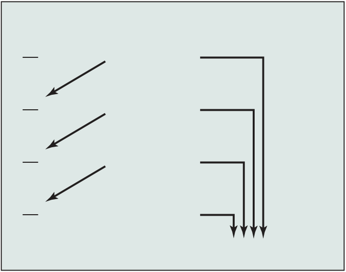
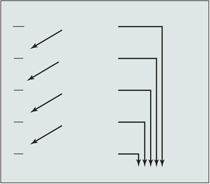
| 21 | = | Quotient | |
|---|---|---|---|
| 10 | |||
| 2 | |||
| 10 | = | 5 |
|
| 2 | |||
| 5 | = | 2 |
|
| 2 | |||
| 2 | = | 1 | |
| 2 | |||
| 1 | = | 0 | |
| 2 |
Figure 9.1 Examples of Converting from Decimal Notation to Binary Notation for Integers
From this equation, we see that the integer part of (2 * F), which must be either 0 or 1 because 0 6 F 6 1, is simply b-1. So we can say (2 * F) = b-1 + F1, where 0 6 F1 6 1 and where
F1 = 2-1* (b-2 + 2-1* (b-3 + 2-1* (b-4 + c) c))
(a) 0.8110 = 0.1100112 (approximately)
| Product | Integer Part | |
|---|---|---|
| 0.25 �� 2 = 0.5 * | 0 | |
| 0.5 �� 2 = 1.0 * | 1 |
Because of the inherent binary nature of digital computer components, all forms of data within computers are represented by various binary codes. However, no matter how convenient the binary system is for computers, it is exceedingly cumbersome for human beings. Consequently, most computer professionals who must spend time working with the actual raw data in the computer prefer a more compact notation.
What notation to use? One possibility is the decimal notation. This is certainly more compact than binary notation, but it is awkward because of the tediousness of converting between base 2 and base 10.
A sequence of hexadecimal digits can be thought of as representing an integer in base 16 (Table 9.3). Thus,
2C16 = (216 * 161) + (C16 * 160)
= (210 * 161) + (1210 * 160) = 44
| (9.4) |
|---|
Table 9.3 Decimal, Binary, and Hexadecimal
326 chaPTeR 9 / NumbeR SySTemS
As an example of the last point, consider the binary string 110111100001. This is equivalent to
| 1101 | 1110 |
|
|---|---|---|
| D | E |
|
|||||||
|---|---|---|---|---|---|---|---|
|
c. 5 | ||||||
| b. 3124 to base 7 | c. 5206 to base 7 |
|
|||||
|
|||||||
| b. 000011 | c. 011100 | d. 111100 | e. 101010 | ||||
|
|
||||||
| c. 111 | d. 145 | ||||||
|
|||||||
| a. 34.75 | b. 25.25 |
|
|||||
Computer ArithmetiC
10.1 The Arithmetic and Logic Unit
10.6 Key Terms, Review Questions, and Problems
328
|
|---|
Computer arithmetic is commonly performed on two very different types of numbers: integer and floating point. In both cases, the representation chosen is a cru-cial design issue and is treated first, followed by a discussion of arithmetic operations.
This chapter includes a number of examples, each of which is highlighted in a shaded box.
330 chApTer 10 / compUTer AriThmeTic
Figure 10.1 ALU Inputs and Outputs
The flag values are also stored in registers within the processor. The processor pro-vides signals that control the operation of the ALU and the movement of the data into and out of the ALU.
| 00000001 =1 |
|---|
| 10000000 = 128 |
|---|
1See Chapter 9 for a basic refresher on number systems (decimal, binary, hexadecimal).
|
|---|
The general case can be expressed as follows:
| A = µ | (10.1) |
|---|
| -010= 10000000(signmagnitude) |
|---|
This is inconvenient because it is slightly more difficult to test for 0 (an operation performed frequently on computers) than if there were a single representation.
Because of these drawbacks, sign-magnitude representation is rarely used in implementing the integer portion of the ALU. Instead, the most common scheme is twos complement representation.2
332 chApTer 10 / compUTer AriThmeTic
Table 10.1 Characteristics of Twos Complement Representation and Arithmetic
Twos Complement A = -2n-1an-1 + a n-2 2iai (10.2) i=0
Equation (10.2) defines the twos complement representation for both positive and negative numbers. For an-1 = 0, the term -2n-1an-1 = 0 and the equation defines
|
|
||
|---|---|---|---|
| +8 | — | — | 1111 |
| +7 | 0111 | 0111 | 1110 |
| +6 | 0110 | 0110 | 1101 |
| +5 | 0101 | 0101 | 1100 |
| +4 | 0100 | 0100 | 1011 |
| +3 | 0011 | 0011 | 1010 |
| +2 | 0010 | 0010 | 1001 |
| +1 | 0001 | 0001 | 1000 |
| +0 | 0000 | 0000 | 0111 |
| -0 | 1000 | — | — |
| -1 | 1001 | 1111 | 0110 |
| -2 | 1010 | 1110 | 0101 |
| -3 | 1011 | 1101 | 0100 |
| -4 | 1100 | 1100 | 0011 |
| -5 | 1101 | 1011 | 0010 |
| -6 | 1110 | 1010 | 0001 |
| -7 | 1111 | 1001 | 0000 |
| -8 | — | 1000 | — |
Range Extension
It is sometimes desirable to take an n-bit integer and store it in m bits, where m 7 n. This expansion of bit length is referred to as range extension, because the range of numbers that can be expressed is extended by increasing the bit length.
| −128 | 64 | 32 | 16 | 8 | 4 | 2 | 1 |
|---|---|---|---|---|---|---|---|
| 1 | 0 | 0 | 0 | 0 | 0 | 1 | 1 |
| −120 =−128 | +8 |
|---|
(c) Convert decimal −120 to binary
Figure 10.2 Use of a Value Box for Conversion between Twos Complement Binary and Decimal
| +18 = | 00010010 | |
|---|---|---|
| +18 = | 0000000000010010 | |
| -18 = | 11101110 |
|
| - 32,658 = | 1000000001101110 |
|
10.3 / inTeger AriThmeTic 335
To see why this rule works, let us again consider an n-bit sequence of bin-ary digits an-1an-2ca1a0 interpreted as a twos complement integer A, so that its value is
The two values must be equal:
-2m-1+ a m-2 2iai = -2n-1+ a n-2 2iai i=0 i=0-2m-1+ m-2 a 2iai = -2n-1
i=n-1Finally, we mention that the representations discussed in this section are sometimes referred to as fixed point. This is because the radix point (binary point) is fixed and assumed to be to the right of the rightmost digit. The programmer can use the same representation for binary fractions by scaling the numbers so that the binary point is implicitly positioned at some other location.
10.3 inTeger AriThmeTic
1. Take the Boolean complement of each bit of the integer (including the sign bit). That is, set each 1 to 0 and each 0 to 1.
2. Treating the result as an unsigned binary integer, add 1.
| 11101110 =-18 |
|---|
| 00010010 =+18 |
|---|
We can demonstrate the validity of the operation just described using the defi-nition of the twos complement representation in Equation (10.2). Again, interpret an n-bit sequence of binary digits an-1an-2ca1a0 as a twos complement integer A, so that its value is
A = -2n-1an-1 + a n-2 2iai
i=0
Now form the bitwise complement, an-1an-2ca0, and, treating this as an unsigned integer, add 1. Finally, interpret the resulting n-bit sequence of binary dig-its as a twos complement integer B, so that its value is
B = -2n-1an-1 + 1 + a n-2 2iai
i=0Now, we want A = -B, which means A + B = 0. This is easily shown to be true: A + B = -(an-1 + an-1)2n-1+ 1 + a a 2i(ai + ai)b
n-2
|
|---|
| 100000000 = 0 |
|---|
There is a carry out of the most significant bit position, which is ignored. The result is that the negation of 0 is 0, as it should be.
| 10000000 =-128 |
|---|
Addition in twos complement is illustrated in Figure 10.3. Addition proceeds as if the two numbers were unsigned integers. The first four examples illustrate successful operations. If the result of the operation is positive, we get a positive number in twos complement form, which is the same as in unsigned-integer form. If the result of the operation is negative, we get a negative number in twos complement form. Note that, in some instances, there is a carry bit beyond the end of the word (indicated by shading), which is ignored.
On any addition, the result may be larger than can be held in the word size being used. This condition is called overflow. When overflow occurs, the ALU must signal this fact so that no attempt is made to use the result. To detect overflow, the following rule is observed:
Figures 10.3e and f show examples of overflow. Note that overflow can occur whether or not there is a carry.
Subtraction is easily handled with the following rule:
Figure 10.4 Subtraction of Numbers in Twos Complement Representation (M - S)
| Subtraction | Addition | Subtraction | 111…1 | Addition | |||||||||||||||||||||
|---|---|---|---|---|---|---|---|---|---|---|---|---|---|---|---|---|---|---|---|---|---|---|---|---|---|
| of positive | of positive | of positive | |||||||||||||||||||||||
| numbers | 1111 | 0000 | numbers |
|
numbers | ||||||||||||||||||||
| 1110 | 0010 | 110…0 | –1 |
|
010…0 | ||||||||||||||||||||
| 1101 | –2 –1 | 0 | +1 | ||||||||||||||||||||||
| –3 | +3 | 2n–2 | |||||||||||||||||||||||
| 1100 | –4 | +4 | |||||||||||||||||||||||
|
–2n–1 |
|
|||||||||||||||||||||||
| –5 | +5 | ||||||||||||||||||||||||
| 1011 | –6 | –7 | –8 | +7 | |||||||||||||||||||||
| 1010 | 0110 | ||||||||||||||||||||||||
| 100…0 | 011…1 | ||||||||||||||||||||||||
| 1001 | 1000 | ||||||||||||||||||||||||
| –9 | –8 | –7 | –6 | –5 | –4 | –3 | –2 | –1 | 0 |
|
|
||||||||||||||
| (a) 4-bit numbers | |||||||||||||||||||||||||
340 chApTer 10 / compUTer AriThmeTic
B Register A Register
Figure 10.6 Block Diagram of Hardware for Addition and Subtraction
data paths. Control signals are needed to control whether or not the complementer is used, depending on whether the operation is addition or subtraction.
|
|
|---|
10.3 / inTeger AriThmeTic 341
Figure 10.8a shows a possible implementation employing these measures. The multiplier and multiplicand are loaded into two registers (Q and M). A third
Multiplicand
| Mn–1 | n-bit adder | M0 | ||
|---|---|---|---|---|
Multiplier
| C | A | Q | M | |||
|---|---|---|---|---|---|---|
| 0 | 0000 | 1101 | 1011 | |||
| 0 | 1011 | 1101 | 1011 | Add | ||
| 0 | 0101 | 1110 | 1011 | Shift | ||
| 0 | 0010 | 1111 | 1011 | Shift |
|
|
| 0 | 1101 | 1111 | 1011 | Add |
|
|
| 0 | 0110 | 1111 | 1011 | Shift | ||
| 1 | 0001 | 1111 | 1011 | Add | ||
| 0 | 1000 | 1111 | 1011 | Shift | ||
Figure 10.8 Hardware Implementation of Unsigned Binary Multiplication
1001
+0011
1100
C, A A + M
Shift right C, A, Q
Count Count – 1
| No | Count = 0? | END | ||
|---|---|---|---|---|
10.3 / inTeger AriThmeTic 343
|
|---|
Unfortunately, this simple scheme will not work for multiplication. To see this, consider again Figure 10.7. We multiplied 11 (1011) by 13 (1101) to get 143 (10001111). If we interpret these as twos complement numbers, we have -5(1011) times -3 (1101) equals -113(10001111). This example demonstrates that straight-forward multiplication will not work if both the multiplicand and multiplier are negative. In fact, it will not work if either the multiplicand or the multiplier is nega-tive. To justify this statement, we need to go back to Figure 10.7 and explain what is being done in terms of operations with powers of 2. Recall that any unsigned binary number can be expressed as a sum of powers of 2. Thus,
1101 = 1 * 23+ 1 * 22+ 0 * 21+ 1 * 20= 23+ 22+ 20
| (a) Unsigned integers |
|
|---|
If the multiplier is negative, straightforward multiplication also will not work. The reason is that the bits of the multiplier no longer correspond to the shifts or multiplications that must take place. For example, the 4-bit decimal number -3 is written 1101 in twos complement. If we simply took partial products based on each bit position, we would have the following correspondence:
1101 4 -(1 * 23+ 1 * 22+ 0 * 21+ 1 * 20) = -(23+ 22+ 20)
A 0, Q�1 0
M Multiplicand
Q Multiplier
Count n
| No | Count � 0? |
|---|
Figure 10.12 Booth’s Algorithm for Twos
Complement Multiplication
respectively. There is also a 1-bit register placed logically to the right of the least significant bit (Q0) of the Q register and designated Q-1; its use is explained shortly. The results of the multiplication will appear in the A and Q registers. A and Q-1 are initialized to 0. As before, control logic scans the bits of the multiplier one at a time. Now, as each bit is examined, the bit to its right is also examined. If the two bits are the same (1–1 or 0–0), then all of the bits of the A, Q, and Q-1 registers are shifted to the right 1 bit. If the two bits differ, then the multiplicand is added to or subtracted from the A register, depending on whether the two bits are 0–1 or 1–0. Following the addition or subtraction, the right shift occurs. In either case, the right shift is such that the leftmost bit of A, namely An-1, not only is shifted into An-2, but also remains in An-1. This is required to preserve the sign of the number in A and Q. It is known as an arithmetic shift, because it preserves the sign bit.
Figure 10.13 shows the sequence of events in Booth’s algorithm for the multi-plication of 7 by 3. More compactly, the same operation is depicted in Figure 10.14a. The rest of Figure 10.14 gives other examples of the algorithm. As can be seen, it works with any combination of positive and negative numbers. Note also the effi-ciency of the algorithm. Blocks of 1s or 0s are skipped over, with an average of only one addition or subtraction per block.
|
|---|
|
|---|
| M * (00011110) = M * (24+ 23+ 22+ 21) |
|---|
| = M * 30 |
|---|
The number of such operations can be reduced to two if we observe that
| M * (00011110) = M * (25- 21) |
|---|
| = M * 30 |
|---|
| = M * (27- 23+ 22- 21) |
|---|
X = -2n-1+ (xn-2 * 2n-2) + (xn-3 * 2n-3) +c(x1 * 21) + (x0 * 20) (10.4)
The reader can verify this by applying the algorithm to the numbers in Table 10.2. The leftmost bit of X is 1, because X is negative. Assume that the leftmost 0 is
10.3 / inTeger AriThmeTic 347
Rearranging
-2n-1+ 2n-2+ 2n-3+c+ 2k+1= -2k+1 (10.7)
| -6 = -27+ 26+ 25+ 24+ 23+ 21 |
|---|
| M * (11111010) = M * ( -27+ 26+ 25+ 24+ 23+ 21) |
|---|
| M * (11111010) = M * ( - 23+ 21) |
|---|
| M * (11111010) = M * ( -23+ 22- 21) |
|---|
Figure 10.15 shows an example of the long division of unsigned binary inte-gers. It is instructive to describe the process in detail. First, the bits of the dividend are examined from left to right, until the set of bits examined represents a number greater than or equal to the divisor; this is referred to as the divisor being able to divide the number. Until this event occurs, 0s are placed in the quotient from left to right. When the event occurs, a 1 is placed in the quotient and the divisor is sub-tracted from the partial dividend. The result is referred to as a partial remainder.
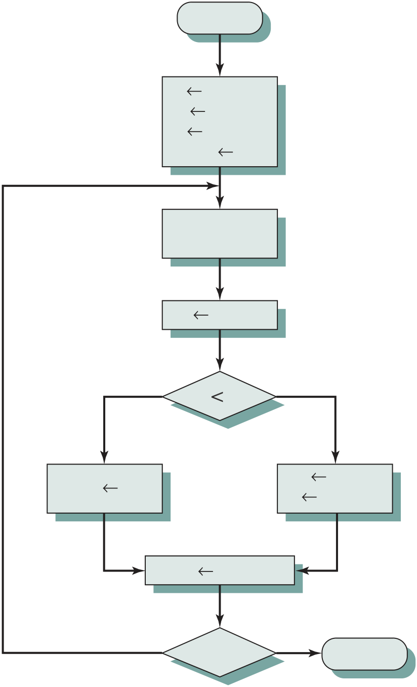
| Partial | 001111 |
|
|---|---|---|
| 1011 | ||
| remainders | ||
| 100 |
Figure 10.15 Example of Division of Unsigned
Binary Integers
Shift left
A, Q
A A � M
| No | Count � 0? |
|
END |
|
|---|---|---|---|---|
A Q
Initial value
Subtract, set Q0 = 1
Shift
This process can, with some difficulty, be extended to negative numbers. We give here one approach for twos complement numbers. An example of this approach is shown in Figure 10.17.
The algorithm assumes that the divisor V and the dividend D are positive and that ∙ V ∙ 6 ∙ D∙. If ∙ V ∙ = ∙ D∙, then the quotient Q = 1 and the remainder R = 0. If ∙ V ∙ 7 ∙ D∙, then Q = 0 and R = D. The algorithm can be summarized as follows:
5. Repeat steps 2 through 4 as many times as there are bit positions in Q.
6. The remainder is in A and the quotient is in Q.
That is, the remainder is the value of R needed for the preceding equation to be valid. Consider the following examples of integer division with all possible com-binations of signs of D and V:
With a fixed-point notation (e.g., twos complement) it is possible to represent a range of positive and negative integers centered on or near 0. By assuming a fixed binary or radix point, this format allows the representation of numbers with a frac-tional component as well.
This approach has limitations. Very large numbers cannot be represented, nor can very small fractions. Furthermore, the fractional part of the quotient in a div-ision of two large numbers could be lost.
■ Sign: plus or minus
■ Significand S
| Sign of | 8 bits | 23 bits |
|---|---|---|
| signifcand | ||
| Signifcand |
(a) Format
1.1010001 × 210100 = 0 10010011 10100010000000000000000 = 1.6328125 × 220–1.1010001 × 210100 = 1 10010011 10100010000000000000000 = –1.6328125 × 220 1.1010001 × 2–10100 = 0 01101011 10100010000000000000000 = 1.6328125 × 2–20–1.1010001 × 2–10100 = 1 01101011 10100010000000000000000 = –1.6328125 × 2–20
Table 10.2 shows the biased representation for 4-bit integers. Note that when the bits of a biased representation are treated as unsigned integers, the relative mag-nitudes of the numbers do not change. For example, in both biased and unsigned representations, the largest number is 1111 and the smallest number is 0000. This is not true of sign-magnitude or twos complement representation. An advantage of biased representation is that nonnegative floating-point numbers can be treated as integers for comparison purposes.
The final portion of the word (23 bits in this case) is the significand.4 Any floating-point number can be expressed in many ways.
| 0.110 * 25 |
|---|

352 chApTer 10 / compUTer AriThmeTic
■ The sign is stored in the first bit of the word.
■ The first bit of the true significand is always 1 and need not be stored in the significand field.
Expressible integers
| Negative | Number line | ||||
|---|---|---|---|---|---|
| underfow | |||||
| Negative |
|
Expressible positive | Positive | ||
| overfow | numbers | Zero |
|
overfow | |
 |
|||||
■ Negative numbers less than - (2 - 2-23) * 2128, called negative overflow■ Negative numbers greater than 2-127, called negative underflow
■ Zero
Also, note that the numbers represented in floating-point notation are not spaced evenly along the number line, as are fixed-point numbers. The possible val-ues get closer together near the origin and farther apart as you move away, as shown in Figure 10.20. This is one of the trade-offs of floating-point math: Many calcula-tions produce results that are not exact and have to be rounded to the nearest value that the notation can represent.
In the type of format depicted in Figure 10.18, there is a trade-off between range and precision. The example shows 8 bits devoted to the exponent and 23 to the significand. If we increase the number of bits in the exponent, we expand the range of expressible numbers. But because only a fixed number of different values can be expressed, we have reduced the density of those numbers and therefore the precision. The only way to increase both range and precision is to use more bits. Thus, most computers offer, at least, single-precision numbers and doublepreci-sion numbers. For example, a processor could support a single-precision format of 64 bits, and a double-precision format of 128 bits.
| �n | 0 | n | 2n | 4n |
|---|
|
|---|
■ Arithmetic format: All the mandatory operations defined by the standard are supported by the format. The format may be used to represent floating-point operands or results for the operations described in the standard.
■ Basic format: This format covers five floating-point representations, three binary and two decimal, whose encodings are specified by the standard, and which can be used for arithmetic. At least one of the basic formats is imple-mented in any conforming implementation.
10.4 / FLoATing-poinT represenTATion 355
8 bits 23 bits
11 bits 52 bits
exponent Trailing signifcand feld
length of the exponent and significand. These formats are arithmetic format types
but not interchange format types. The extended formats are to be used for inter-
| Parameter | Format | ||
|---|---|---|---|
| Binary32 | Binary64 | Binary128 | |
| 32 | 64 | 128 | |
| 8 | 11 | 15 | |
|
127 | 1023 | 16383 |
|
127 | 1023 | 16383 |
| -126 | -1022 | -16382 | |
| 10-38,10+38 | 10-308,10+308 | 10-4932,10+4932 | |
| 23 | 52 | 112 | |
| 254 | 2046 | 32766 | |
|
223 | 252 | 2112 |
|
1.98 * 231 | 1.99 * 263 | 1.99 * 2128 |
| 2-126 | 2-1022 | 2-16362 | |
| 2128- 2104 | 21024- 2971 | 216384- 216271 | |
| 2-149 | 2-1074 | 2-16494 | |
356 chApTer 10 / compUTer AriThmeTic
chance of a final result that has been contaminated by excessive roundoff error; with their greater range, they also lessen the chance of an intermediate overflow aborting a computation whose final result would have been representable in a basic format. An additional motivation for the extended format is that it affords some of the benefits of a larger basic format without incurring the time penalty usually associated with higher precision.
■ An exponent of zero together with a fraction of zero represents positive or negative zero, depending on the sign bit. As was mentioned, it is useful to have an exact value of 0 represented.
Table 10.4 IEEE Formats
10.4 / FLoATing-poinT represenTATion 357
Table 10.5 Interpretation of IEEE 754 Floating-Point Numbers
| Sign | Biased Exponent | Fraction | value | |
|---|---|---|---|---|
| 0 | 0 | 0 | 0 | |
| 1 | 0 | 0 | -0 | |
| 0 | all 1s | 0 | ∞ | |
|
1 | all 1s | 0 | -∞ |
|
0 or 1 | all 1s | ≠ 0;firstbit = 1 | qNaN |
| 0 or 1 | all 1s | ≠ 0;firstbit = 0 | sNaN | |
| 0 | 0 6 e 6 225 | f | 2e-127(1.f) | |
| 1 | 0 6 e 6 225 | f | -2e-127(1.f) | |
| 0 | 0 | f ≠ 0 | 2e-126(0.f) | |
|
1 | 0 | f ≠ 0 | -2e-126(0.f) |
(b) binary64 format
(c) binary128 format
| Sign | Biased Exponent | Fraction | value | |
|---|---|---|---|---|
|
0 | 0 | 0 | 0 |
| 1 | 0 | 0 | -0 | |
| 0 | all 1s | 0 | ∞ | |
| 1 | all 1s | 0 | - ∞ | |
| 0 or 1 | all 1s | ≠ 0;firstbit = 1 | qNaN | |
|
0 or 1 | all 1s | ≠ 0;firstbit = 0 | sNaN |
|
0 | all 1s | f | 2e-16383(1.f) |
| 1 | all 1s | f | -2e-16383(1.f) | |
| 0 | 0 | f ≠ 0 | 2e-16383(0.f) | |
| 1 | 0 | f ≠ 0 | -2e-16383(0.f) |
■ An exponent of all ones together with a fraction of zero represents positive or negative infinity, depending on the sign bit. It is also useful to have a represen-tation of infinity. This leaves it up to the user to decide whether to treat over-flow as an error condition or to carry the value ∞ and proceed with whatever program is being executed.
■ An exponent of zero together with a nonzero fraction represents a subnormal number. In this case, the bit to the left of the binary point is zero and the true exponent is -126 or -1022. The number is positive or negative depending on the sign bit.
A floating-point operation may produce one of these conditions:
■ Exponent overflow: A positive exponent exceeds the maximum possible expo- nent value. In some systems, this may be designated as +∞ or - ∞.
Examples:
X * Y = (0.3 * 0.2) * 102+3= 0.06 * 105= 6000
X , Y = (0.3 , 0.2) * 102-3= 1.5 * 10-1= 0.15
In floating-point arithmetic, addition and subtraction are more complex than multi-plication and division. This is because of the need for alignment. There are four basic phases of the algorithm for addition and subtraction:
1. Check for zeros.
Phase 1. Zero check: Because addition and subtraction are identical except for a sign change, the process begins by changing the sign of the subtrahend if it is a subtract operation. Next, if either operand is 0, the other is reported as the result.
Phase 2. Significand alignment: The next phase is to manipulate the numbers so that the two exponents are equal.
| Clearly, we cannot just add the significands. The digits must first be set into equivalent |
|---|
| these conditions, the two exponents will be equal, which is the mathematical condition |
|---|
| (123 * 100) + (456 * 10-2) = (123 * 100) + (4.56 * 100) = 127.56 * 100 |
|---|
RETURN
| RETURN | Report | Yes | Exponent | |
|---|---|---|---|---|
| overfow | overfow? |
Phase 3. Addition: Next, the two significands are added together, taking into account their signs. Because the signs may differ, the result may be 0. There is also the possibility of significand overflow by 1 digit. If so, the significand of the result is shifted right and the exponent is incremented. An exponent overflow could occur as a result; this would be reported and the operation halted.
Phase 4. Normalization: The final phase normalizes the result. Normalization consists of shifting significand digits left until the most significant digit (bit, or 4 bits for base-16 exponent) is nonzero. Each shift causes a decrement of the exponent and thus could cause an exponent underflow. Finally, the result must be rounded off and then reported. We defer a discussion of rounding until after a discussion of multiplication and division.
After the product is calculated, the result is then normalized and rounded, as was done for addition and subtraction. Note that normalization could result in exponent underflow.
Finally, let us consider the flowchart for division depicted in Figure 10.24. Again, the first step is testing for 0. If the divisor is 0, an error report is issued, or the result is set to infinity, depending on the implementation. A dividend of 0 results in 0. Next, the divisor exponent is subtracted from the dividend exponent. This removes the bias, which must be added back in. Tests are then made for expo-nent underflow or overflow.
| Exponent | Yes | |
|---|---|---|
| overfow? |
|
No
Normalize
Round RETURN
| The reason for the use of guard bits is illustrated in Figure 10.25. Consider numbers in |
|---|
10.5 / FLoATing-poinT AriThmeTic 363
| X � 0? | No | Y � 0? | No | |
|---|---|---|---|---|
| Yes | ||||
| Z 0 | Z � |
|
RETURN
| Exponent | Yes | |
|---|---|---|
| underfow? |
|
No
Figure 10.24 Floating-Point Division (Z d X/Y)
| (c) Hexadecimal example, without guard bits |
|---|
|
(d) Hexadecimal example, with guard bits |
|---|
Figure 10.25 The Use of Guard Bits
rounding Another detail that affects the precision of the result is the rounding policy. The result of any operation on the significands is generally stored in a longer register. When the result is put back into the floating-point format, the extra bits must be eliminated in such a way as to produce a result that is close to the exact result. This process is called rounding.
A number of techniques have been explored for performing rounding. In fact, the IEEE standard lists four alternative approaches:
| If the extra bits, beyond the 23 bits that can be stored, are 10010, then the extra bits |
|---|
|
|---|
10.5 / FLoATing-poinT AriThmeTic 365
The next two options, rounding to plus and minus infinity, are useful in imple-menting a technique known as interval arithmetic. Interval arithmetic provides an efficient method for monitoring and controlling errors in floating-point computa-tions by producing two values for each result. The two values correspond to the lower and upper endpoints of an interval that contains the true result. The width of the interval, which is the difference between the upper and lower endpoints, indi-cates the accuracy of the result. If the endpoints of an interval are not representa-ble, then the interval endpoints are rounded down and up, respectively. Although the width of the interval may vary according to implementation, many algorithms have been designed to produce narrow intervals. If the range between the upper and lower bounds is sufficiently narrow, then a sufficiently accurate result has been obtained. If not, at least we know this and can perform additional analysis.
- ∞6 (everyfinitenumber) 6 +∞
With the exception of the special cases discussed subsequently, any arithmetic operation involving infinity yields the obvious result.
quietandsignalingnans A NaN is a symbolic entity encoded in floating-point format, of which there are two types: signaling and quiet. A signaling NaN signals an invalid operation exception whenever it appears as an operand. Signaling
| Operation | Quiet NaN Produced By |
|---|---|
| Any | Any operation on a signaling NaN |
| Add or subtract |
|
| Multiply |
|
| Division | |
| Remainder | x REM 0 or ∞ REM y |
| Square root | x, where x 6 0 |
Gap
| 0 | 2−126 | 2−124 | 2−123 |
|---|
(b) 32-bit format with subnormal numbers
Figure 10.26 The Effect of IEEE 754 Subnormal Numbers
Key Terms
|
|---|
10.6
|
|
|---|
10.10
10.22 |
||||||||
|---|---|---|---|---|---|---|---|---|
| b. | -6 + 13 | c. 6 - 13 | d. | |||||
| a. | 111000 |
|
c. | 111100001111 | d. | 11000011 | ||
|
||||||||
|
||||||||
370 chApTer 10 / compUTer AriThmeTic
|
|
|---|
10.40 |
|
|
|---|---|---|
|
||
a. (2.255 * 101) * (1.234 * 100)
11.1 Boolean Algebra
11.2 Gates
372
11.1 / Boolean algeBra 373
The operation of the digital computer is based on the storage and processing of binary data. Throughout this book, we have assumed the existence of storage ele-ments that can exist in one of two stable states, and of circuits than can operate on binary data under the control of control signals to implement the various computer functions. In this chapter, we suggest how these storage elements and circuits can be implemented in digital logic, specifically with combinational and sequential circuits. The chapter begins with a brief review of Boolean algebra, which is the mathemati-cal foundation of digital logic. Next, the concept of a gate is introduced. Finally, com-binational and sequential circuits, which are constructed from gates, are described.
■ Design: Given a desired function, Boolean algebra can be applied to develop a simplified implementation of that function.
As with any algebra, Boolean algebra makes use of variables and operations. In this case, the variables and operations are logical variables and operations. Thus, a variable may take on the value 1 (TRUE) or 0 (FALSE). The basic logical
NOTA = A
The operation AND yields true (binary value 1) if and only if both of its operands are true. The operation OR yields true if either or both of its operands are true. The unary operation NOT inverts the value of its operand. For example, consider the
| D = A + (B#C) |
|---|
Table 11.1a defines the basic logical operations in a form known as a truth table, which lists the value of an operation for every possible combination of val-ues of operands. The table also lists three other useful operators: XOR, NAND, and NOR. The exclusive- or (XOR) of two logical operands is 1 if and only if exactly one of the operands has the value 1. The NAND function is the complement (NOT) of the AND function, and the NOR is the complement of OR:
ANANDB = NOT(AANDB) = AB
2Logical NOT is often indicated by an apostrophe: NOT A = A′.
11.1 / Boolean algeBra 375
| Expression | Output = 1if | |
|---|---|---|
|
||
|
||
|
||
|
||
|
The two bottommost expressions are referred to as DeMorgan’s theorem. We can restate them as follows:
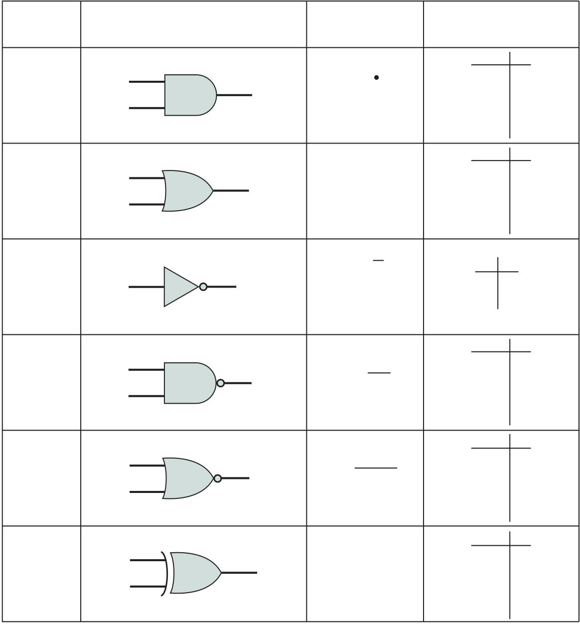
Each gate shown in Figure 11.1 has one or two inputs and one output. How-ever, as indicated in Table 11.1b, all of the gates except NOT can have more than two inputs. Thus, (X + Y + Z) can be implemented with a single OR gate with three inputs. When one or more of the values at the input are changed, the correct output signal appears almost instantaneously, delayed only by the propagation time of signals through the gate (known as the gate delay). The significance of this delay is discussed in Section 11.3. In some cases, a gate is implemented with two outputs, one output being the negation of the other output.
| Name | A |
|
Algebraic | |||
|---|---|---|---|---|---|---|
| Function | ||||||
| AND | F | F = A • B | A B | |||
| 0 | 0 | |||||
| B | or | 0 | 1 | |||
| 1 | 0 |
|
||||
| F = AB | ||||||
| 1 | 1 |
|
||||
| OR | A | F | F = A + B | A B | ||
| 0 | 0 | |||||
| 0 | 1 | |||||
| B | ||||||
| 1 | 0 | |||||
| NOT | A | F | F = A | 1 | 1 |
|
| A |
|
|||||
| 0 | ||||||
| or | ||||||
| 1 | ||||||
| F = A′ | ||||||
| NAND | A | F | F = AB | A B | ||
| 0 | 0 | |||||
| 0 | 1 |
|
||||
| B | ||||||
| 1 | 0 |
|
||||
| 1 | 1 | |||||
| XOR |
|
F | F = A ⊕ B |
|
|---|---|---|---|---|
| B | ||||
11.2 / gaTes 377
■ OR, NOT
■ NAND
Figure 11.2 shows how the AND, OR, and NOT functions can be implemented solely with NAND gates, and Figure 11.3 shows the same thing for NOR gates. For this reason, digital circuits can be, and frequently are, implemented solely with NAND gates or solely with NOR gates.
Figure 11.2 Some Uses of NAND Gates

| A | A | ||
|---|---|---|---|
|
A+B | ||
|
|||
A combinational circuit is an interconnected set of gates whose output at any time is a function only of the input at that time. As with a single gate, the appearance of the input is followed almost immediately by the appearance of the output, with only gate delays.
In general terms, a combinational circuit consists of n binary inputs and m binary outputs. As with a gate, a combinational circuit can be defined in three ways:
Any Boolean function can be implemented in electronic form as a network of gates. For any given function, there are a number of alternative realizations. Consider the Boolean function represented by the truth table in Table 11.3. We can express this function by simply itemizing the combinations of values of A, B, and C that cause F to be 1:
F + ABC + ABC + ABC (11.1)
There are three combinations of input values that cause F to be 1, and if any one of these combinations occurs, the result is 1. This form of expression, for self- evident reasons, is known as the sum of products (SOP) form. Figure 11.4 shows a straightfor-ward implementation with AND, OR, and NOT gates.
Figure 11.4 Sum- of- Products Implementation of Table 11.3
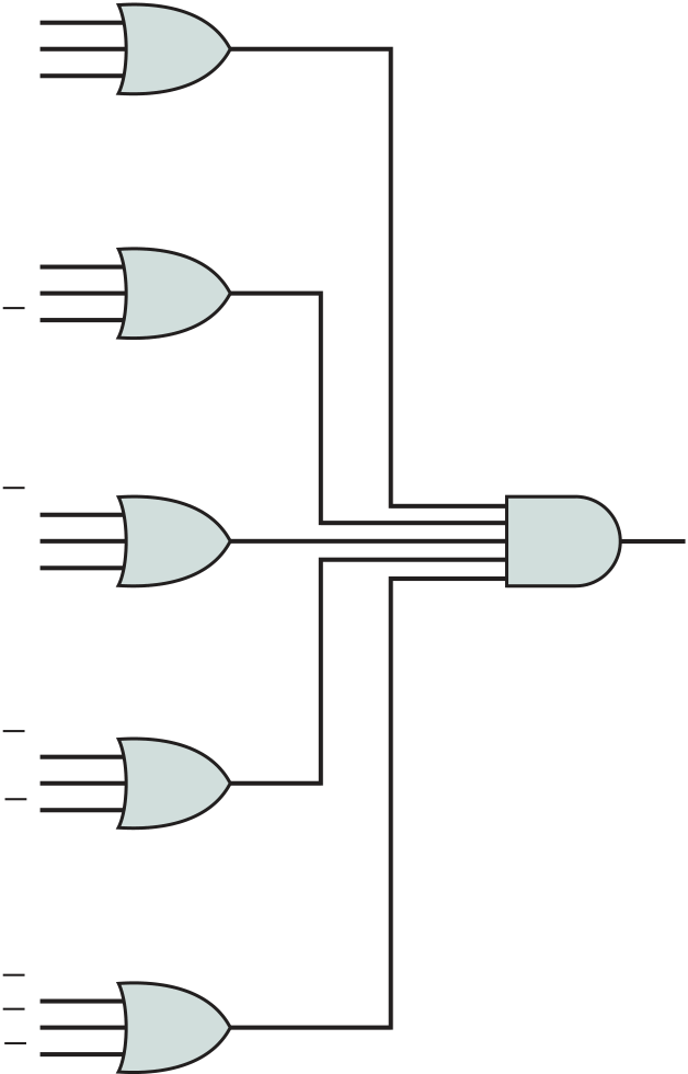
| F |
|---|
A
B
CA
B
C■ It is often possible to derive a simpler Boolean expression from the truth table than either SOP or POS.
■ It may be preferable to implement the function with a single gate type (NAND or NOR).
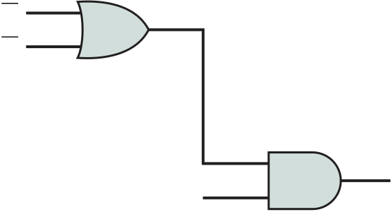
11.3 / ComBinaTional CirCuiTs 381
This expression can be implemented as shown in Figure 11.6. The simplification of Equation (11.1) was done essentially by observation. For more complex expres-sions, some more systematic approach is needed.
karnaughmaps For purposes of simplification, the Karnaugh map is a convenient way of representing a Boolean function of a small number (up to four) of variables. The map is an array of 2n squares, representing all possible combinations of values of n binary variables. Figure 11.7a shows the map of four squares for a function of two variables. It is essential for later purposes to list the combinations in the order 00, 01, 11, 10. Because the squares corresponding to the combinations are to be used for recording information, the combinations are customarily written above the squares. In the case of three variables, the representation is an arrangement of eight squares (Figure 11.7b), with the values for one of the variables to the left and for the other two variables above the squares. For four variables, 16 squares are needed, with the arrangement indicated in Figure 11.7c.
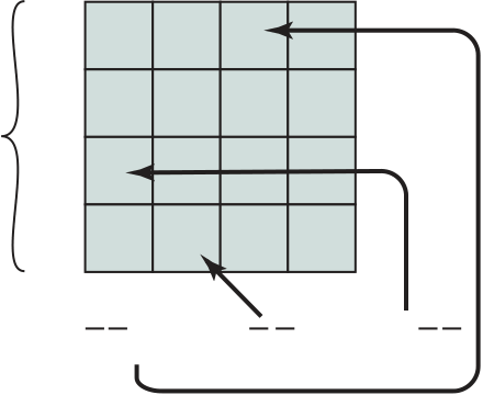
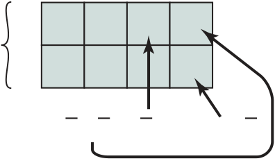
382 CHaPTer 11 / DigiTal logiC
AB BC
| 00 | 01 | 11 | A | 0 | 00 | 01 | 11 | ||
|---|---|---|---|---|---|---|---|---|---|
| 1 | 1 | 1 | |||||||
| (a) F = AB + AB | 1 |
|
|||||||
(b) F = ABC + ABC + ABC
D
(d) Simplifed labeling of mapFigure 11.7 The Use of Karnaugh Maps to Represent Boolean Functions
We can summarize the rules for simplification as follows:
1. Among the marked squares (squares with a 1), find those that belong to a unique largest block of 1, 2, 4, or 8 and circle those blocks.
Figure 11.8 The Use of Karnaugh Maps
BC
CD
An example, presented in [HAYE98], illustrates the points we have been dis-cussing. We would like to develop the Boolean expressions for a circuit that adds 1 to a packed decimal digit. For packed decimal, each decimal digit is represented by a 4-bit code, in the obvious way. Thus, 0 = 0000,1 = 0001, c,8 = 1000, and 9 = 1001. The remaining 4-bit values, from 1010 to 1111, are not used. This code is also referred to as Binary Coded Decimal (BCD).
Table 11.4 shows the truth table for producing a 4-bit result that is one more than a 4-bit BCD input. The addition is modulo 10. Thus, 9 + 1 = 0. Also, note that six of the input codes produce “don’t care” results, because those are not valid BCD inputs. Figure 11.10 shows the resulting Karnaugh maps for each of the output variables. The d squares are used to achieve the best possible groupings.
tables in four dimensions! An alternative approach is a tabular technique, referred to as the Quine– McCluskey method. The method is suitable for programming on a computer to give an automatic tool for producing minimized Boolean expressions.
Figure 11.10 Karnaugh Maps for the Incrementer
The first step is to construct a table in which each row corresponds to one of the product terms of the expression. The terms are grouped according to the number of complemented variables. That is, we start with the term with no comple-ments, if it exists, then all terms with one complement, and so on. Table 11.5 shows the list for our example expression, with horizontal lines used to indicate the group-ing. For clarity, each term is represented by a 1 for each uncomplemented variable and a 0 for each complemented variable. Thus, we group terms according to the number of 1s they contain. The index column is simply the decimal equivalent and is useful in what follows.
The next step is to find all pairs of terms that differ in only one variable, that is, all pairs of terms that are the same except that one variable is 0 in one of the terms and 1 in the other. Because of the way in which we have grouped the terms, we can do this by starting with the first group and comparing each term of the first group with every term of the second group. Then compare each term of the second group with all of the terms of the third group, and so on. Whenever a match is found, place a check next to each term, combine the pair by eliminating the variable that differs in the two terms, and add that to a new list. Thus, for example, the terms ABCD and ABCD are combined to produce ABC. This process continues until the entire ori-ginal table has been examined. The result is a new table with the following entries:
Table 11.5 First Stage of Quine– McCluskey Method
(forF = ABCD + ABCD + ABCD + ABCD + ABCD + ABCD + ABCD + ABCD)
|
||||||
|---|---|---|---|---|---|---|
The new table is organized into groups, as indicated, in the same fashion as the first table. The second table is then processed in the same manner as the first. That is, terms that differ in only one variable are checked and a new term produced for a third table. In this example, the third table that is produced contains only one term: BD.
In general, the process would proceed through successive tables until a table with no matches was produced. In this case, this has involved three tables.
ABC + ABC = AB(C + C) = AB
After the elimination of variables, we are left with an expression that is clearly equivalent to the original expression. However, there may be redundant terms in this expression, just as we found redundant groupings in Karnaugh maps. The mat-rix layout assures that each term in the original expression is covered and does so in a way that minimizes the number of terms in the final expression.
B
C
Because the complement of the complement of a value is just the original value,
F = B(A + C) = (AB + (BC)
The multiplexer connects multiple inputs to a single output. At any time, one of the inputs is selected to be passed to the output. A general block diagram representation is shown in Figure 11.12. This represents a 4- to- 1 multiplexer. There are four input lines, labeled D0, D1, D2, and D3. One of these lines is selected to provide the output
|
|||
|---|---|---|---|
These various inputs could be connected to the input lines of a multiplexer, with the PC connected to the output line. The select lines determine which value is loaded into the PC. Because the PC contains multiple bits, multiple multiplexers are used, one per bit. Figure 11.14 illustrates this for 16-bit addresses.
Decoders
| Chip | |
|---|---|
|
Each chip requires 8 address lines, and these are supplied by the lower- order 8 bits of the address. The higher- order 2 bits of the 10-bit address are used to select one of the four RAM chips. For this purpose, a 2- to- 4 decoder is used whose output enables one of the four chips, as shown in Figure 11.16.
B
001 D1
101 D5
110 D6
| 2-to-4 |
|
|
||
|---|---|---|---|---|
| RAM |
|
|||
| Enable | Enable | Enable | Enable | |
| Decoder |
A8
392 CHaPTer 11 / DigiTal logiC
n-bit
Read- Only Memory
Combinational circuits are often referred to as “memoryless” circuits, because their output depends only on their current input and no history of prior inputs is retained. However, there is one sort of memory that is implemented with combinational cir-cuits, namely read- only memory (ROM).
Binary addition differs from Boolean algebra in that the result includes a carry term. Thus,
Table 11.8 Truth Table for a ROM
| (b) Addition with Carry Input | |||||
|---|---|---|---|---|---|
|
|||||
For a multiple- bit adder to work, each of the single- bit adders must have three inputs, including the carry from the next- lower- order adder. The revised truth table appears in Table 11.9b. The two outputs can be expressed:
Sum = ABC + ABC + ABC + ABC
| Overfow | C3 | A3 | S3 | B3 | C2 | A2 | S2 | B2 | C1 | A1 | S1 | B1 |
|
C0 | A0 | S0 | B0 |
|
0 | ||
|---|---|---|---|---|---|---|---|---|---|---|---|---|---|---|---|---|---|---|---|---|---|
| signal |
A
B
C
B
C
| A | 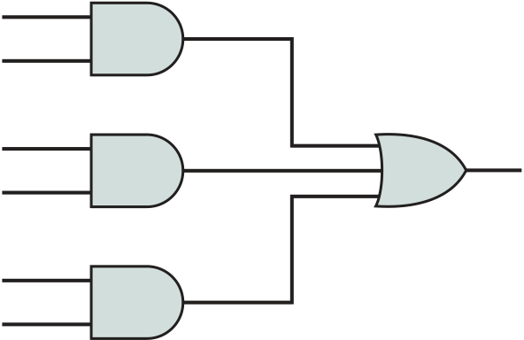 |
|
|---|---|---|
| B | ||
| A | ||
| C | ||
| B | ||
| C |
If the carry values could be determined without having to ripple through all the previous stages, then each single- bit adder could function independently, and delay would not accumulate. This can be achieved with an approach known as carry lookahead. Let us look again at the 4-bit adder to explain this approach.
We would like to come up with an expression that specifies the carry input to any stage of the adder without reference to previous carry values. We have
Figure 11.21 Construction of a 32-Bit Adder Using 8-Bit Adders
396 CHaPTer 11 / DigiTal logiC
This process can be repeated for arbitrarily long adders. Each carry term can be expressed in SOP form as a function only of the original inputs, with no dependence on the carries. Thus, only two levels of gate delay occur regardless of the length of the adder.
For long numbers, this approach becomes excessively complicated. Evaluating the expression for the most significant bit of an n- bit adder requires an OR gate with 2n-1 inputs and 2n-1 AND gates with from 2 to n + 1 inputs. Accordingly, full carry lookahead is typically done only 4 to 8 bits at a time. Figure 11.21 shows how a 32-bit adder can be constructed out of four 8-bit adders. In this case, the carry must ripple through the four 8-bit adders, but this will be substantially quicker than a ripple through thirty- two 1-bit adders.
The simplest form of sequential circuit is the flip- flop. There are a variety of flip- flops, all of which share two properties:
■ The flip- flop is a bistable device. It exists in one of two states and, in the absence of input, remains in that state. Thus, the flip- flop can function as a 1-bit memory.
| S |
|
Q |
|---|---|---|
| Q |
Figure 11.22 The S– R Latch Implemented with NOR Gates
clockeds– rflip- flop The output of the S– R latch changes, after a brief time delay, in response to a change in the input. This is referred to as asynchronous operation. More typically, events in the digital computer are synchronized to a clock pulse, so that changes occur only when a clock pulse occurs. Figure 11.24 shows this
| Q |
|
∆t | 2∆t |
|---|
0
Figure 11.23 NOR S– R Latch Timing Diagram
| (b) Simplified Characteristic Table | |||
|---|---|---|---|
|
|||
| R | Q |
|---|
Q
Clock
| Q |
|---|
The D flip- flop is sometimes referred to as the data flip- flop because it is, in effect, storage for one bit of data. The output of the D flip- flop is always equal to the most recent value applied to the input. Hence, it remembers and produces the last input. It is also referred to as the delay flip- flop, because it delays a 0 or 1 applied to its input for a single clock pulse. We can capture the logic of the D flip- flop in the following truth table:
K
Figure 11.26 J– K Flip- Flop
| Name | Graphical Symbol | Truth Table | ||||||
|---|---|---|---|---|---|---|---|---|
| S–R |
|
|
||||||
| J–K | Ck
|
|||||||
| D |
|
11.4 / sequenTial CirCuiTs 401
Data lines
Clock
Load
ments of the CPU: the register. As we know, a register is a digital circuit used within
the CPU to store one or more bits of data. Two basic types of registers are commonly
The 8-bit register of Figure 11.28 illustrates the operation of a parallel register
using D flip- flops. A control signal, labeled load, controls writing into the register
from clocked D flip- flops. Data are input only to the leftmost flip- flop. With each
clock pulse, data are shifted to the right one position, and the rightmost bit is
| Serial in | D | Q | D | Q | D | Q | D | Q | D | Q | Serial out |
|---|---|---|---|---|---|---|---|---|---|---|---|
|
|
402 CHaPTer 11 / DigiTal logiC
ripplecounter An asynchronous counter is also referred to as a ripple counter, because the change that occurs to increment the counter starts at one end and “ripples” through to the other end. Figure 11.30 shows an implementation of a 4-bit counter using J– K flip- flops, together with a timing diagram that illustrates its behavior. The timing diagram is idealized in that it does not show the propagation delay that occurs as the signals move down the series of flip- flops. The output of the leftmost flip- flop (Q0) is the least significant bit. The design could clearly be extended to an arbitrary number of bits by cascading more flip- flops.
High
(a) Sequential circuit
Q3
(b) Timing diagram
For a 3-bit counter, three flip- flops will be needed. Let us use J– K flip- flops. Label the uncomplemented output of the three flip- flops C, B, and A, respectively, with C representing the most significant bit. The first step is to construct a truth table that relates the J– K inputs and outputs, to allow us to design the overall cir-cuit. Such a truth table is shown in Figure 11.31a. The first three columns show the possible combinations of outputs C, B, and A. They are listed in the order that they will appear as the counter is incremented. Each row lists the current value of C, B, and A and the inputs to the three flip- flops that will be required to reach the next value of C, B, and A.
To understand the way in which the truth table of Figure 11.31a is constructed, it may be helpful to recast the characteristic table for the J– K flip- flop. Recall that this table was presented as follows:
| Qn+1 | |
|---|---|
|
|
404 CHaPTer 11 / DigiTal logiC
|
0 | (a) Truth table | C | B | A Jc | Kc | Jb | Kb | |||||||||||||||||||||||||||||
|---|---|---|---|---|---|---|---|---|---|---|---|---|---|---|---|---|---|---|---|---|---|---|---|---|---|---|---|---|---|---|---|---|---|---|---|---|---|
| BA | BA | ||||||||||||||||||||||||||||||||||||
| 00 | 01 | 11 | 10 | 00 | 01 | 11 | |||||||||||||||||||||||||||||||
| Jc = BA | C |
|
Kc = BA | C | 0 | ||||||||||||||||||||||||||||||||
| 1 | 1 | ||||||||||||||||||||||||||||||||||||
| Jb = A | C | 0 | BA | BA | |||||||||||||||||||||||||||||||||
| 00 | 01 | 11 | 10 | 00 | 01 | 11 | |||||||||||||||||||||||||||||||
|
Kb = A | C | 0 | ||||||||||||||||||||||||||||||||||
| 1 | 1 | ||||||||||||||||||||||||||||||||||||
| Ja = 1 | C | 0 | BA | BA | |||||||||||||||||||||||||||||||||
| 00 | 01 | 11 | 10 | 00 | 01 | 11 | 10 | ||||||||||||||||||||||||||||||
|
Ka = 1 | 0 | |||||||||||||||||||||||||||||||||||
| 1 | 1 | ||||||||||||||||||||||||||||||||||||
(c) Logic diagram
| Ck | Ck | Ck | C | output | ||
|---|---|---|---|---|---|---|
| Ka | Kb | Kc |
Figure 11.31 Design of a Synchronous Counter
Let us return to Figure 11.31a. Consider the first row. We want the value of C to remain 0, the value of B to remain 0, and the value of A to go from 0 to 1 with the next application of a clock pulse. The excitation table shows that to maintain an output of 0, we must have inputs of J = 0 and don’t care for K. To effect a transition from 0 to 1, the inputs must be J = 1 and K = d. These values are shown in the first row of the table. By similar reasoning, the remainder of the table can be filled in.
As the level of integration provided by integrated circuits increases, other considerations apply. Early integrated circuits, using small- scale integration (SSI), provided from one to ten gates on a chip. Each gate is treated independently, in the building- block approach described so far. To construct a logic function, a number of these chips are laid out on a printed circuit board and the appropriate pin intercon-nections are made.
Increasing levels of integration made it possible to put more gates on a chip and to make gate interconnections on the chip as well. This yields the advantages of decreased cost, decreased size, and increased speed (because on- chip delays are of shorter duration than off- chip delays). A design problem arises, however. For each particular logic function or set of functions, the layout of gates and interconnec-tions on the chip must be designed. The cost and time involved in such custom chip design is high. Thus, it becomes attractive to develop a general- purpose chip that can be readily adapted to specific purposes. This is the intent of the programmable logic device (PLD).
406 CHaPTer 11 / DigiTal logiC
Table 11.11 PLD Terminology
Figure 11.32b shows a programmed PLA that realizes two Boolean expressions.
Field- Programmable Gate Array
| I1 | I2 |
|---|
“AND” array
| ABC + AB |
|
|---|
Figure 11.32 An Example of a Programmable Logic Array (PLA)
■ Logic block: The configurable logic blocks are where the computation of the user’s circuit takes place.
■ I/O block: The I/O blocks connect I/O pins to the circuitry on the chip.
| A0 | D |
|
2-to-1 | |
|---|---|---|---|---|
| MUX | ||||
| A1 | ||||
| A2 | Ck | |||
| A3 |
Clock
Problems
|
|---|
410 CHaPTer 11 / DigiTal logiC
|
|
||||||||||||||||||
|---|---|---|---|---|---|---|---|---|---|---|---|---|---|---|---|---|---|---|---|
| BCD | Z2 | Z1 | |||||||||||||||||
| x1 | Z4 | ||||||||||||||||||
| x2 | |||||||||||||||||||
|
|||||||||||||||||||
| digit | x3 | Z5 |
|
||||||||||||||||
| x4 | |||||||||||||||||||
| (a) | |||||||||||||||||||
(b)
Figure 11.35 Seven- Segment LED Display Example
11.6 / Key Terms anD ProBlems 411
11.15 |
|
|---|
| 11.16 11.17 |
|
|---|


12.2 Types of Operands
Numbers
Characters
Logical Data12.3 Intel x86 and ARM Data Types
x86 Data Types
ARM Data Types
| 412 |
|---|
12.1 / Machine instruction characteristics 413
Much of what is discussed in this book is not readily apparent to the user or pro-grammer of a computer. If a programmer is using a high- level language, such as Pascal or Ada, very little of the architecture of the underlying machine is visible.
Elements of a Machine Instruction
Each instruction must contain the information required by the processor for execu-tion. Figure 12.1, which repeats Figure 3.6, shows the steps involved in instruction execution and, by implication, defines the elements of a machine instruction. These elements are as follows:
| Instruction | Operand | Data |
|
|
|---|---|---|---|---|
| fetch | fetch |
|
||
| Instruction | Multiple | Multiple | ||
| operands | results | |||
| Instruction | ||||
| address | operation | address | ||
| calculation | decoding |
|
|
|
Figure 12.1 Instruction Cycle State Diagram
■ Result operand reference: The operation may produce a result.
■ Processor register: With rare exceptions, a processor contains one or more registers that may be referenced by machine instructions. If only one register exists, reference to it may be implicit. If more than one register exists, then each register is assigned a unique name or number, and the instruction must contain the number of the desired register.
■ Immediate: The value of the operand is contained in a field in the instruction being executed.
| Opcode | Operand reference | Operand reference |
|---|
ADD Add
SUB Subtract
Operands are also represented symbolically. For example, the instruction
ADD R, Y
and so on. A simple program would accept this symbolic input, convert opcodes and operand references to binary form, and construct binary machine instructions.
Machine- language programmers are rare to the point of nonexistence. Most programs today are written in a high- level language or, failing that, assembly lan-guage, which is discussed in Appendix B. However, symbolic machine language remains a useful tool for describing machine instructions, and we will use it for that purpose.
This statement instructs the computer to add the value stored in Y to the value stored in X and put the result in X. How might this be accomplished with machine instructions? Let us assume that the variables X and Y correspond to locations 513 and 514. If we assume a simple set of machine instructions, this operation could be accomplished with three instructions:
1. Load a register with the contents of memory location 513.
■ Data processing: Arithmetic and logic instructions.
■ Data storage: Movement of data into or out of register and or memory locations.
12.1 / Machine instruction characteristics 417
Figure 12.3 compares typical one-, two-, and three- address instructions that could be used to compute Y = (A - B)/[C + (D * E)]. With three addresses, each instruction specifies two source operand locations and a destination operand location. Because we choose not to alter the value of any of the operand locations,
| Instruction |
|
Instruction | ||||||||
|---|---|---|---|---|---|---|---|---|---|---|
| SUB | Y, A, B | Y | ||||||||
| MPY | T, D, E | T | ||||||||
| ADD | T |
|
||||||||
| DIV | Y, Y, T | Y |
|
|||||||
| Instruction | LOAD D | AC | ||||||||
| MPY | E | AC | ||||||||
| ADD | C | AC |
|
|||||||
| MOVE Y, A | Y |
|
||||||||
| STOR Y | Y | |||||||||
| SUB | Y, B | Y | ||||||||
| LOAD A | AC | |||||||||
| MOVE T, D | T | |||||||||
| SUB | B | AC |
|
|||||||
| MPY | T, E | T |
|
|||||||
| DIV | Y | AC | ||||||||
| ADD | T | |||||||||
| STOR Y | Y | |||||||||
| DIV | Y, T | Y |
|
|||||||
(b) Two-address instructions |
||||||||||
a temporary location, T, is used to store some intermediate results. Note that there are four instructions and that the original expression had five operands.
Three- address instruction formats are not common because they require a relatively long instruction format to hold the three address references. With two- address instructions, and for binary operations, one address must do double duty as both an operand and a result. Thus, the instruction SUB Y, B carries out the calcu-lation Y - B and stores the result in Y. The two- address format reduces the space requirement but also introduces some awkwardness. To avoid altering the value of an operand, a MOVE instruction is used to move one of the values to a result or temporary location before performing the operation. Our sample program expands to six instructions.
Table 12.1 Utilization of Instruction Addresses (Nonbranching Instructions)
The design trade- offs involved in choosing the number of addresses per instruc-tion are complicated by other factors. There is the issue of whether an address refer-ences a memory location or a register. Because there are fewer registers, fewer bits are needed for a register reference. Also, as we will see in Chapter 13, a machine may offer a variety of addressing modes, and the specification of mode takes one or more bits. The result is that most processor designs involve a variety of instruction formats.
Instruction Set Design
■ Instruction format: Instruction length (in bits), number of addresses, size of various fields, and so on.
■ Registers: Number of processor registers that can be referenced by instruc- tions, and their use.
12.2 TYPES OF OPERANDS
Machine instructions operate on data. The most important general categories of data are
We shall see, in discussing addressing modes in Chapter 13, that addresses are, in fact, a form of data. In many cases, some calculation must be performed on the operand reference in an instruction to determine the main or virtual memory address. In this context, addresses can be considered to be unsigned integers.
Other common data types are numbers, characters, and logical data, and each of these is briefly examined in this section. Beyond that, some machines define spe-cialized data types or data structures. For example, there may be machine opera-tions that operate directly on a list or a string of characters.
■ Binary floating point
■ Decimal
With packed decimal, each decimal digit is represented by a 4-bit code, in the obvious way, with two digits stored per byte. Thus, 0 = 000,1 = 0001, c,8 = 1000, and 9 = 1001. Note that this is a rather inefficient code because only 10 of 16 possible 4-bit values are used. To form numbers, 4-bit codes are strung together, usually in multiples of 8 bits. Thus, the code for 246 is 0000 0010 0100 0110. This code is clearly less compact than a straight binary representation, but it avoids the conversion overhead. Negative numbers can be represented by including a 4-bit sign digit at either the left or right end of a string of packed decimal digits. Standard sign values are 1100 for positive ( + ) and 1101 for negative ( - ).
Many machines provide arithmetic instructions for performing operations directly on packed decimal numbers. The algorithms are quite similar to those described in Section 9.3 but must take into account the decimal carry operation.
Logical Data
Normally, each word or other addressable unit (byte, halfword, and so on) is treated as a single unit of data. It is sometimes useful, however, to consider an n- bit unit as consisting of n 1-bit items of data, each item having the value 0 or 1. When data are viewed this way, they are considered to be logical data.
x86 Data Types
The x86 can deal with data types of 8 (byte), 16 (word), 32 (doubleword), 64 (quad-word), and 128 (double quadword) bits in length. To allow maximum flexibility in data structures and efficient memory utilization, words need not be aligned at even- numbered addresses; doublewords need not be aligned at addresses evenly divisible by 4; quadwords need not be aligned at addresses evenly divisible by 8; and so on. However, when data are accessed across a 32-bit bus, data transfers take place in units of doublewords, beginning at addresses divisible by 4. The processor converts the request for misaligned values into a sequence of requests for the bus transfer. As with all of the Intel 80x86 machines, the x86 uses the little- endian style; that is, the least significant byte is stored in the lowest address (see Appendix 12A for a discus-sion of endianness).
■ Packed word and packed word integer: 16-bit words packed into a 64-bit quad-word or 128-bit double quadword, interpreted as a bit field or as an integer.
12.3 / inteL x86 and arM data tyPes 423
■ Packed doubleword and packed doubleword integer: 32-bit doublewords packed into a 64-bit quadword or 128-bit double quadword, interpreted as a bit field or as an integer.
■ Packed quadword and packed quadword integer: Two 64-bit quadwords packed into a 128-bit double quadword, interpreted as a bit field or as an integer.
– The address is treated as truncated, with address bits[1:0] treated as zero for word accesses, and address bit[0] treated as zero for halfword accesses.
424 chaPter 12 / instruction sets: characteristics and Functions
| exp | signif icand |
|---|
|
signif icand |
|---|
– Load single word ARM instructions are architecturally defined to rotate right the word- aligned data transferred by a non word- aligned address one, two, or three bytes depending on the value of the two least significant address bits.
■ Alignment checking: When the appropriate control bit is set, a data abort sig- nal indicates an alignment fault for attempting unaligned access.
12.4 / tyPes oF oPerations 425
Data bytes
in memory
(ascending address values
from byte 0 to byte 3)
|
|
||||||||
|---|---|---|---|---|---|---|---|---|---|
| Byte 3 | Byte 2 | Byte 1 | Byte 0 | Byte 1 | Byte 2 | ||||
| ARM register | ARM register | ||||||||
|
Program status register E-bit = 1 | ||||||||
Figure 12.5 ARM Endian Support— Word Load/Store with E- Bit
■ Arithmetic
■ Logical
Table 12.3 (based on [HAYE98]) lists common instruction types in each cat-egory. This section provides a brief survey of these various types of operations, together with a brief discussion of the actions taken by the processor to execute a particular type of operation (summarized in Table 12.4). The latter topic is exam-ined in more detail in Chapter 14.
Table 12.3 Common Instruction Set Operations
| Type | Operation Name | Description |
|---|---|---|
|
|
|
| Transfer instructions to I/O processor to initiate I/O operation | ||
|
||
|
||
Table 12.4 Processor Actions for Various Types of Operations
The most fundamental type of machine instruction is the data transfer instruction. The data transfer instruction must specify several things. First, the location of the source and destination operands must be specified. Each location could be memory, a register, or the top of the stack. Second, the length of data to be transferred must be indicated. Third, as with all instructions with operands, the mode of addressing for each operand must be specified. This latter point is discussed in Chapter 13.
The choice of data transfer instructions to include in an instruction set exem-plifies the kinds of trade- offs the designer must make. For example, the general location (memory or register) of an operand can be indicated in either the specifica-tion of the opcode or the operand. Table 12.5 shows examples of the most common IBM EAS/390 data transfer instructions. Note that there are variants to indicate
| Name | Description | ||
|---|---|---|---|
|
|
32 | |
| 16 | |||
|
|
32 | |
| 32 | |||
|
|
32 | |
| 64 | |||
|
|
64 | |
| 32 | |||
|
|
16 | |
| 8 | |||
|
|
32 | |
| 64 |
the amount of data to be transferred (8, 16, 32, or 64 bits). Also, there are different instructions for register to register, register to memory, memory to register, and memory to memory transfers. In contrast, the VAX has a move (MOV) instruction with variants for different amounts of data to be moved, but it specifies whether an operand is register or memory as part of the operand. The VAX approach is some-what easier for the programmer, who has fewer mnemonics to deal with. However, it is also somewhat less compact than the IBM EAS/390 approach because the loca-tion (register versus memory) of each operand must be specified separately in the instruction. We will return to this distinction when we discuss instruction formats in Chapter 13.
In terms of processor action, data transfer operations are perhaps the simplest type. If both source and destination are registers, then the processor simply causes data to be transferred from one register to another; this is an operation internal to the processor. If one or both operands are in memory, then the processor must per-form some or all of the following actions:
12.4 / tyPes oF oPerations 429
Arithmetic
■ Increment: Add 1 to the operand.
■ Decrement: Subtract 1 from the operand.
These logical operations can be applied bitwise to n- bit logical data units.
Thus, if two registers contain the data
Table 12.6 Basic Logical Operations
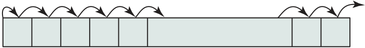
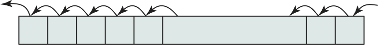
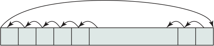
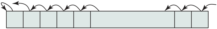
then
(R1) XOR (R2) = 01011010
(a) Logical right shift
0
0
S • • •
(f) Left rotate
Figure 12.6 Shift and Rotate Operations
3. Perform I/O. The I/O module reads the lower- order 8 bits from the data bus.
The preceding steps result in sending the left- hand character. To send the right- hand character;
Rotate, or cyclic shift, operations preserve all of the bits being operated on. One use of a rotate is to bring each bit successively into the leftmost bit, where it can be identified by testing the sign of the data (treated as a number).
As with arithmetic operations, logical operations involve ALU activity and may involve data transfer operations. Table 12.7 gives examples of all of the shift and rotate operations discussed in this subsection.
| Input | Operation | Result |
|---|---|---|
| 10100110 | 00010100 | |
| 10100110 | 00110000 | |
| 10100110 | 11110100 | |
| 10100110 |
|
10110000 |
| 10100110 |
|
11010100 |
| 10100110 | 00110101 |
TR R1 (L), R2
The operand R2 contains the address of the start of a table of 8-bit codes. The L bytes starting at the address specified in R1 are translated, each byte being replaced by the contents of a table entry indexed by that byte. For example, to translate from EBCDIC to IRA, we first create a 256-byte table in storage locations, say, 1000-10FF hexadecimal. The table contains the characters of the IRA code in the sequence of the binary representation of the EBCDIC code; that is, the IRA code is placed in the table at the relative location equal to the binary value of the EBCDIC code of the same character. Thus, locations 10F0 through 10F9 will contain the val-ues 30 through 39, because F0 is the EBCDIC code for the digit 0, and 30 is the IRA code for the digit 0, and so on through digit 9. Now suppose we have the EBCDIC for the digits 1984 starting at location 2100 and we wish to translate to IRA. Assume the following:
TR R1 (4), R2
locations 2100–2103 will contain 31 39 38 34.
Some examples of system control operations are as follows. A system con-trol instruction may read or alter a control register; we discuss control registers in Chapter 14. Another example is an instruction to read or modify a storage protec-tion key, such as is used in the EAS/390 memory system. Yet another example is access to process control blocks in a multiprogramming system.
12.4 / tyPes oF oPerations 433
One sequence of instructions is executed repeatedly to process all the data. 2. Virtually all programs involve some decision making. We would like the computer to do one thing if one condition holds, and another thing if another condition holds. For example, a sequence of instructions computes the square root of a num- ber. At the start of the sequence, the sign of the number is tested. If the number is negative, the computation is not performed, but an error condition is reported.
3. To compose correctly a large or even medium- size computer program is an exceedingly difficult task. It helps if there are mechanisms for breaking the task up into smaller pieces that can be worked on one at a time.
| Unconditional | Memory | |||
|---|---|---|---|---|
| address | ||||
202
|
||||
| branch | ||||
| 211 | ||||
| 225 | ||||
|
||||
| 235 | ||||
BRE R1, R2, X Branch to X if contents of R1 = contents of R2.
Figure 12.7 shows examples of these operations. Note that a branch can be either forward (an instruction with a higher address) or backward (lower address). The example shows how an unconditional and a conditional branch can be used to create a repeating loop of instructions. The instructions in locations 202 through 210 will be executed repeatedly until the result of subtracting Y from X is 0.
In this fragment, the two transfer- of- control instructions are used to implement an iterative loop. R1 is set with the negative of the number of iterations to be performed. At the end of the loop, R1 is incremented. If it is not 0, the program branches back to the beginning of the loop. Otherwise, the branch is skipped, and the program continues with the next instruction after the end of the loop.
12.4 / tyPes oF oPerations 435
| Addresses | Main memory |
|
|
|---|---|---|---|
| 4000 | |||
| 4500 |
|
|
|
| 4800 | |||
|
|||
| (a) Calls and returns | (b) Execution sequence |
Figure 12.8 Nested Procedures
2. A procedure call can appear in a procedure. This allows the nesting of proce- dures to an arbitrary depth.
3. Each procedure call is matched by a return in the called program.
Consider a machine- language instruction CALL X, which stands for call procedure at location X. If the register approach is used, CALL X causes the following actions:
RN d PC + ∆
PC d XThis is quite handy. The return address has been stored safely away.
Both of the preceding approaches work and have been used. The only limita-tion of these approaches is that they complicate the use of reentrant procedures. A reentrant procedure is one in which it is possible to have several calls open to it at the same time. A recursive procedure (one that calls itself) is an example of the use of this feature (see Appendix M). If parameters are passed via registers or memory for a reentrant procedure, some code must be responsible for saving the parameters so that the registers or memory space are available for other procedure calls.
Figure 12.9 Use of Stack to Implement Nested Subroutines of Figure 12.8
| y2 |
|---|
y1
12.5 INTEL x86 AND ARM OPERATION TYPES
x86 Operation Types
■ Copy the stack pointer as the new value of the frame pointer.
■ Adjust the stack pointer to allocate a frame.
The ENTER instruction was added to the instruction set to provide direct sup-port for the compiler. The instruction also includes a feature for support of what are called nested procedures in languages such as Pascal, COBOL, and Ada (not found in C or FORTRAN). It turns out that there are better ways of handling nested pro-cedure calls for these languages. Furthermore, although the ENTER instruction
12.5 / inteL x86 and arM oPeration tyPes 439
Table 12.8 lists the status flags used on the x86. Each flag, or combinations of these flags, can be tested for a conditional jump. Table 12.9 shows the condition codes (combinations of status flag values) for which conditional jump opcodes have been defined.
Several interesting observations can be made about this list. First, we may wish to test two operands to determine if one number is bigger than another. But this will depend on whether the numbers are signed or unsigned. For example, the 8-bit number 11111111 is bigger than 00000000 if the two numbers are interpreted
|
Comment | |
|---|---|---|
|
||
| AE, NB, NC | ||
|
|
|
| Below or equal; Not above (less than or equal, unsigned) | ||
|
|
|
|
|
|
|
|
|
|
|
|
|
|
|
|
|
|
A second observation concerns the complexity of comparing signed integers. A signed result is greater than or equal to zero if (1) the sign bit is zero and there is no overflow (S = 0 AND O = 0), or (2) the sign bit is one and there is an overflow. A study of Figure 10.4 should convince you that the conditions tested for the vari-ous signed operations are appropriate.
x86 simdinstructions In 1996, Intel introduced MMX technology into its Pentium product line. MMX is set of highly optimized instructions for multimedia tasks. There are 57 new instructions that treat data in a SIMD ( single- instruction, multiple- data) fashion, which makes it possible to perform the same operation, such as addition or multiplication, on multiple data elements at once. Each instruction typically takes a single clock cycle to execute. For the proper application, these fast parallel operations can yield a speedup of two to eight times over comparable algorithms that do not use the MMX instructions [ATKI96]. With the introduction of 64-bit x86 architecture, Intel has expanded this extension to include double
■ Packed word: Four 16-bit words packed into 64 bits.
■ Packed doubleword: Two 32-bit doublewords packed into 64 bits.
F000h = 1111000000000000
+ 3000h = 0011000000000000
10010000000000000
1111111111111111 = FFFFh
To provide a feel for the use of MMX instructions, we look at an example, taken from [PELE97]. A common video application is the fade- out, fade- in effect, in which one scene gradually dissolves into another. Two images are combined with a weighted average:
12.5 / inteL x86 and arM oPeration tyPes 443
instructions executed using MMX is 535 million. The same calculation, performed without the MMX instructions, requires 1.4 billion instruction executions [INTE98].
ARM Operation Types
■ Multiply instructions: The integer multiply instructions operate on word or halfword operands and can produce normal or long results. For example, there is a multiply instruction that takes two 32-bit operands and produces a 64-bit result.
■ Parallel addition and subtraction instructions: In addition to the normal data processing and multiply instructions, there are a set of parallel addition and subtraction instructions, in which portions of two operands are operated on in parallel. For example, ADD16 adds the top halfwords of two registers to form the top halfword of the result and adds the bottom halfwords of the same two registers to form the bottom halfword of the result. These instructions are useful in image processing applications, similar to the x86 MMX instructions.
Table 12.11 ARM Conditions for Conditional Instruction Execution
| Code | Symbol | Condition Tested | Comment |
|---|---|---|---|
| 0000 |
|
||
| 0001 |
|
||
| 0010 |
|
||
| 0011 |
|
||
| 0100 |
|
||
| 0101 |
|
||
| 0110 |
|
||
| 0111 |
|
||
| 1000 |
|
||
| 1001 |
|
||
| 1010 |
|
||
| 1011 |
|
||
| 1100 |
|
||
| 1101 |
|
||
| 1110 |
|
||
| 1111 |
|
x86 architecture. These four flags constitute a condition code in ARM. Table 12.11 shows the combination of conditions for which conditional execution is defined.
446 chaPter 12 / instruction sets: characteristics and Functions
12.6 KEY TERMS, REVIEW QUESTIONS, AND PROBLEMS
Review Questions
|
|
|---|
12.6 |
|
|---|
for each of the four machines. The instructions available for use are as follows:
| 12.7 | Consider a hypothetical computer with an instruction set of only two n- bit instruc-tions. The first bit specifies the opcode, and the remaining bits specify one of the 2n-1
|
|
|---|---|---|
| SUBS X | ||
b. Addition: Add contents of location X to accumulator.
c. Conditional branch.
|
|---|
12.15 |
|
|---|
12.6 / Key terMs, review Questions, and ProbLeMs 449
A: = (B 7 C) OR (D = F)
A compiler might generate the following code:
| N1 | MOV | ||
|---|---|---|---|
|
|||
| MOV |
|
||
| MOV |
|
||
|
|||
| MOV | |||
| N2 | EAX, F | ||
| MOV | |||
|
|||
| MOV |
|
||
| BL, BH |
450 chaPter 12 / instruction sets: characteristics and Functions
12.21 12.22 |
|
|---|
} s1;
b. struct {
short i; //0x1112
short j; //0x1314
12.6 / Key terMs, review Questions, and ProbLeMs 451
| 12.26 12.27 |
|---|
mem d LoadMemory(…)
byte d VirtualAddress1..0
if CONDITION then
GPR[rt] d 024}mem31 – 8*byte .. 24 – 8*byte else
GPR[rt] d 024}mem7 + 8*byte .. 8*byte endifwhere byte refers to the two low- order bits of the effective address and mem refers to the value loaded from memory. In the manual, instead of the word CONDITION, one of the following two words is used: BigEndian, LittleEndian. Which word is used?
APENDIX 12A LITTLE-, BIG-, AND BI- ENDIAN
An annoying and curious phenomenon relates to how the bytes within a word and the bits within a byte are both referenced and represented. We look first at the prob-lem of byte ordering and then consider that of bits.
| Address | Address |
|
|||||
|---|---|---|---|---|---|---|---|
| 184 |
|
184 | |||||
| 185 | 185 | ||||||
| 186 | 186 | ||||||
| 187 | 187 |
The mapping on the left stores the most significant byte in the lowest numerical byte address; this is known as big endian and is equivalent to the left- to- right order of writing in Western culture languages. The mapping on the right stores the least significant byte in the lowest numerical byte address; this is known as little endian and is reminiscent of the right- to- left order of arithmetic operations in arithmetic units.3 For a given multibyte scalar value, big endian and little endian are byte- reversed mappings of each other.
aPendiX 12a / LittLe-, biG-, and bi- endian 453
struct{
char d[7]; //'A','B','C','D','E','F','G' byte array
short e; //0x5152 halfword
lower left results from compilation of that structure for a big- endian machine, and that
in the lower right for a little- endian machine. In each case, memory is depicted as a
ory assignment. In fact, in looking at programmer manuals for a variety of machines,
a bewildering collection of depictions is to be found, even within the same manual.
char* c; //0x3132_3334 word
char d[7]; //'A','B','C','D','E','F','G' byte array
■ Each data item has the same address in both schemes. For example, the address
of the doubleword with hexadecimal value 2122232425262728 is 08.
The effect of endianness is perhaps more clearly demonstrated when we view memory as a vertical array of bytes, as shown in Figure 12.14.
There is no general consensus as to which is the superior style of endianness.4 The following points favor the big- endian style:
0C 10 |
|
00 04 18 1C |
|||||||||||||||||||||||||||||||||||||
|---|---|---|---|---|---|---|---|---|---|---|---|---|---|---|---|---|---|---|---|---|---|---|---|---|---|---|---|---|---|---|---|---|---|---|---|---|---|---|---|
| (a) Big endian | |||||||||||||||||||||||||||||||||||||||
aPendiX 12a / LittLe-, biG-, and bi- endian 455
■ Decimal/IRA dumps: All values can be printed left to right without causing confusion.
The differences are minor and the choice of endian style is often more a matter of accommodating previous machines than anything else.
The PowerPC is a bi- endian processor that supports both big- endian and little- endian modes. The bi- endian architecture enables software developers to choose either mode when migrating operating systems and applications from other machines. The operating system establishes the endian mode in which processes execute. Once a mode is selected, all subsequent memory loads and stores are determined by the memory- addressing model of that mode. To support this hardware feature, 2 bits are maintained in the machine state register (MSR) maintained by the operating system as part of the process state. One bit specifies the endian mode in which the kernel runs; the other specifies the processor’s current operating mode. Thus, mode can be changed on a per- process basis.
These questions are not answered in the same way on all machines. Indeed, on some machines, the answers are different in different circumstances. Furthermore, the choice of big- or little- endian bit ordering within a byte is not always consistent with big- or little- endian ordering of bytes within a multibyte scalar. The program-mer needs to be concerned with these issues when manipulating individual bits.
Another area of concern is when data are transmitted over a bit- serial line. When an individual byte is transmitted, does the system transmit the most significant bit first or the least significant bit first? The designer must make certain that incom-ing bits are handled properly. For a discussion of this issue, see [JAME90].
13.2 x86 and ARM Addressing Modes
x86 Addressing Modes
ARM Addressing Modes13.3 Instruction Formats
Instruction Length
Allocation of Bits
Variable- Length Instructions
13.1 / Addressing Modes 457
In Chapter 12, we focused on what an instruction set does. Specifically, we examined the types of operands and operations that may be specified by machine instructions. This chapter turns to the question of how to specify the operands and operations of instructions. Two issues arise. First, how is the address of an operand specified, and second, how are the bits of an instruction organized to define the operand addresses and operation of that instruction?
■ Indirect
■ Register
A = contents of an address field in the instruction
R = contents of an address field in the instruction that refers to a register EA = actual (effective) address of the location containing the referenced operand (X) = contents of memory location X or register X
Memory |
Operand (c) Indirect |
|||
|---|---|---|---|---|
Memory
|
|
|||
(g) Stack |
||||
13.1 / Addressing Modes 459
Table 13.1 Basic Addressing Modes
Immediate Addressing
Direct Addressing
A very simple form of addressing is direct addressing, in which the address field con-tains the effective address of the operand:
EA = (A)
460 CHAPTer 13 / insTruCTion seTs: Addressing Modes And ForMATs
In this case, one bit of a full- word address is an indirect flag (I). If the I bit is 0, then the word contains the EA. If the I bit is 1, then another level of indirection is invoked. There does not appear to be any particular advantage to this approach, and its disadvantage is that three or more memory references could be required to fetch an operand.
Register Addressing
If register addressing is heavily used in an instruction set, this implies that the processor registers will be heavily used. Because of the severely limited number of registers (compared with main memory locations), their use in this fashion makes sense only if they are employed efficiently. If every operand is brought into a regis-ter from main memory, operated on once, and then returned to main memory, then a wasteful intermediate step has been added. If, instead, the operand in a register remains in use for multiple operations, then a real savings is achieved. An example is the intermediate result in a calculation. In particular, suppose that the algorithm
13.1 / Addressing Modes 461
EA = (R)
The advantages and limitations of register indirect addressing are basically the same as for indirect addressing. In both cases, the address space limitation (limited range of addresses) of the address field is overcome by having that field refer to a word- length location containing an address. In addition, register indirect addressing uses one less memory reference than indirect addressing.
We will describe three of the most common uses of displacement addressing:
■ Relative addressing
462 CHAPTer 13 / insTruCTion seTs: Addressing Modes And ForMATs
base- registeraddressing For base- register addressing, the interpretation is the following: The referenced register contains a main memory address, and the address field contains a displacement (usually an unsigned integer representation) from that address. The register reference may be explicit or implicit.
EA = A + (R)
(R) d (R) + 1In some machines, both indirect addressing and indexing are provided, and it is possible to employ both in the same instruction. There are two possibilities: the indexing is performed either before or after the indirection.
With preindexing, the indexing is performed before the indirection:
EA = (A + (R))
The stack mode of addressing is a form of implied addressing. The machine instructions need not include a memory reference but implicitly operate on the top of the stack.
13.2 x86 AND ARM ADDRESSING MODES
464 CHAPTer 13 / insTruCTion seTs: Addressing Modes And ForMATs
|
|||
|---|---|---|---|
| SS | Selector | ||
| GS | |||
| FS |
|
||
| ES |
|
||
| DS | |||
| CS | |||
For the immediate mode, the operand is included in the instruction. The oper-and can be a byte, word, or doubleword of data.
For register operand mode, the operand is located in a register. For general instructions, such as data transfer, arithmetic, and logical instructions, the operand can be one of the 32-bit general registers (EAX, EBX, ECX, EDX, ESI, EDI, ESP, EBP), one of the 16-bit general registers (AX, BX, CX, DX, SI, DI, SP, BP), or one of the 8-bit general registers (AH, BH, CH, DH, AL, BL, CL, DL). There are also some instructions that reference the segment selector registers (CS, DS, ES, SS, FS, GS).
| Algorithm | |
|---|---|
|
The remaining addressing modes are indirect, in the sense that the address portion of the instruction tells the processor where to look to find the address. The base mode specifies that one of the 8-, 16-, or 32-bit registers contains the effective address. This is equivalent to what we have referred to as register indirect addressing.
In the base with displacement mode, the instruction includes a displacement to be added to a base register, which may be any of the general- purpose registers.
■ Used to access a field of a record. The base register points to the beginning of the record, while the displacement is an offset to the field.
In the scaled index with displacement mode, the instruction includes a dis-placement to be added to a register, in this case called an index register. The index register may be any of the general- purpose registers except the one called ESP, which is generally used for stack processing. In calculating the effective address, the contents of the index register are multiplied by a scaling factor of 1, 2, 4, or 8, and then added to a displacement. This mode is very convenient for indexing arrays. A scaling factor of 2 can be used for an array of 16-bit integers. A scaling factor of 4 can be used for 32-bit integers or floating- point numbers. Finally, a scaling factor of 8 can be used for an array of double- precision floating- point numbers.
Typically, a RISC machine, unlike a CISC machine, uses a simple and relatively straightforward set of addressing modes. The ARM architecture departs somewhat from this tradition by providing a relatively rich set of addressing modes. These modes are most conveniently classified with respect to the type of instruction.1
load/storeaddressing Load and store instructions are the only instructions that reference memory. This is always done indirectly through a base register plus offset. There are three alternatives with respect to indexing (Figure 13.3):
STRB r0, [r1, #12]
| Original | r1 | Offset | 0x20C | r0 | ||
|---|---|---|---|---|---|---|
| 0xC | ||||||
| 0x200 | 0x5 | register | ||||
| for STR | ||||||
| base register |
STRB r0, [r1], #12
| Updated | r1 | Offset | 0x20C | r0 |
|
|
|---|---|---|---|---|---|---|
| 0xC | ||||||
| base register | ||||||
| Original | r1 | 0x200 | 0x5 | register | ||
| for STR | ||||||
| base register |
468 CHAPTer 13 / insTruCTion seTs: Addressing Modes And ForMATs
load/storemultipleaddressing Load Multiple instructions load a subset (possibly all) of the general- purpose registers from memory. Store Multiple instructions store a subset (possibly all) of the general- purpose registers to memory. The list of registers for the load or store is specified in a 16-bit field in the instruction with each bit corresponding to one of the 16 registers. Load and Store Multiple addressing modes produce a sequential range of memory addresses. The lowest- numbered register is stored at the lowest memory address and the highest- numbered register at the highest memory address. Four addressing modes are used (Figure 13.4): increment after, increment before, decrement after, and decrement before. A base
LDMxx r10, {r0, r1, r4}
Figure 13.4 ARM Load/Store Multiple Addressing
13.3 / insTruCTion ForMATs 469
An instruction format defines the layout of the bits of an instruction, in terms of its constituent fields. An instruction format must include an opcode and, implicitly or explicitly, zero or more operands. Each explicit operand is referenced using one of the addressing modes described in Section 13.1. The format must, implicitly or explicitly, indicate the addressing mode for each operand. For most instruction sets, more than one instruction format is used.
The design of an instruction format is a complex art, and an amazing variety of designs have been implemented. We examine the key design issues, looking briefly at some designs to illustrate points, and then we examine the x86 and ARM solu-tions in detail.
470 CHAPTer 13 / insTruCTion seTs: Addressing Modes And ForMATs
A seemingly mundane but nevertheless important feature is that the instruc-tion length should be a multiple of the character length, which is usually 8 bits, and of the length of fixed- point numbers. To see this, we need to make use of that unfor-tunately ill- defined word, word [FRAI83]. The word length of memory is, in some sense, the “natural” unit of organization. The size of a word usually determines the size of fixed- point numbers (usually the two are equal). Word size is also typ-ically equal to, or at least integrally related to, the memory transfer size. Because a common form of data is character data, we would like a word to store an inte-gral number of characters. Otherwise, there are wasted bits in each word when storing multiple characters, or a character will have to straddle a word boundary. The importance of this point is such that IBM, when it introduced the System/360 and wanted to employ 8-bit characters, made the wrenching decision to move from the 36-bit architecture of the scientific members of the 700/7000 series to a 32-bit architecture.
■ Number of addressing modes: Sometimes an addressing mode can be indi-cated implicitly. For example, certain opcodes might always call for indexing. In other cases, the addressing modes must be explicit, and one or more mode bits will be needed.
■ Number of operands: We have seen that fewer addresses can make for longer, more awkward programs (e.g., Figure 12.3). Typical instruction formats on today’s machines include two operands. Each operand address in the instruc-tion might require its own mode indicator, or the use of a mode indicator could be limited to just one of the address fields.
■ Address range: For addresses that reference memory, the range of addresses that can be referenced is related to the number of address bits. Because this imposes a severe limitation, direct addressing is rarely used. With displacement addressing, the range is opened up to the length of the address register. Even so, it is still convenient to allow rather large displacements from the register address, which requires a relatively large number of address bits in the instruction.
■ Address granularity: For addresses that reference memory rather than registers, another factor is the granularity of addressing. In a system with 16- or 32-bit words, an address can reference a word or a byte at the designer’s choice. Byte addressing is convenient for character manipulation but requires, for a fixed- size memory, more address bits.
Figure 13.5 shows the PDP- 8 instruction format. There are a 3-bit opcode and three types of instructions. For opcodes 0 through 5, the format is a single- address
472 CHAPTer 13 / insTruCTion seTs: Addressing Modes And ForMATs
| Opcode | D/I | Z/C | Displacement |
|---|
| 0 | 2 | 8 | 9 | 11 | |
|---|---|---|---|---|---|
| Group 1 microinstructions |
|
||||
| CLA | CLL | CMA | CML | RAR | RAL | BSW | IAC |
|---|
| 0 | 1 | 2 | 3 | 4 | 5 | 6 | 7 | 8 | 9 | 10 | 11 |
|---|
| CLA | MQA | 0 | MQL | 0 | 0 | 0 | 1 |
|---|
D/I = Direct/Indirect address
Z/C = Page 0 or Current page
CLA = Clear Accumulator
CLL = Clear Link
CMA = CoMplement Accumulator CML = CoMplement Link
RAR = Rotate Accumulator Right RAL = Rotate Accumulator Left BSW = Byte SWapIAC = Increment ACcumulator
SMA = Skip on Minus Accumulator
SZA = Skip on Zero Accumulator
SNL = Skip on Nonzero Link
RSS = Reverse Skip Sense
OSR = Or with Switch Register
HLT = HaLT
MQA= Multiplier Quotient into Accumulator MQL = Multiplier Quotient LoadAmong the design principles employed in designing the instruction set were the following [BELL78c]:
■ Orthogonality: Orthogonality is a principle by which two variables are inde- pendent of each other. In the context of an instruction set, the term indicates
Each of these principles advances the main goal of ease of programming.
The PDP- 10 has a 36-bit word length and a 36-bit instruction length. The fixed instruction format is shown in Figure 13.6. The opcode occupies 9 bits, allow-ing up to 512 operations. In fact, a total of 365 different instructions are defined. Most instructions have two addresses, one of which is one of 16 general- purpose registers. Thus, this operand reference occupies 4 bits. The other operand refer-ence starts with an 18-bit memory address field. This can be used as an immedi-ate operand or a memory address. In the latter usage, both indexing and indirect addressing are allowed. The same general- purpose registers are also used as index registers.
| Opcode | Register | I |
|
Memory address |
|---|
474 CHAPTer 13 / insTruCTion seTs: Addressing Modes And ForMATs
The principal price to pay for variable- length instructions is an increase in the complexity of the processor. Falling hardware prices, the use of microprogramming (discussed in Part Four), and a general increase in understanding the principles of processor design have all contributed to making this a small price to pay. However, we will see that RISC and superscalar machines can exploit the use of fixed- length instructions to provide improved performance.
PDP- 11 instructions are usually one word (16 bits) long. For some instruc-tions, one or two memory addresses are appended, so that 32-bit and 48-bit instruc-tions are part of the repertoire. This provides for further flexibility in addressing.
The PDP- 11 instruction set and addressing capability are complex. This increases both hardware cost and programming complexity. The advantage is that more efficient or compact programs can be developed.
13.3 / insTruCTion ForMATs 475
Numbers below felds indicate bit length.
The result is a highly variable instruction format. An instruction consists of a 1- or 2-byte opcode followed by from zero to six operand specifiers, depending on the opcode. The minimal instruction length is 1 byte, and instructions up to 37 bytes can be constructed. Figure 13.8 gives a few examples.
The VAX instruction begins with a 1-byte opcode. This suffices to handle most VAX instructions. However, as there are over 300 different instructions, 8 bits are not enough. The hexadecimal codes FD and FF indicate an extended opcode, with the actual opcode being specified in the second byte.
|
|
|
|---|---|---|
which is signaled by the pattern 00 in the leftmost 2 bits, leaving space for a 6-bit literal. Because of this exception, a total of 12 different addressing modes can be specified.
An operand specifier often consists of just one byte, with the rightmost 4 bits specifying one of 16 general- purpose registers. The length of the operand specifier can be extended in one of two ways. First, a constant value of one or more bytes may immediately follow the first byte of the operand specifier. An example of this is the displacement mode, in which an 8-, 16-, or 32-bit displacement is used. Second, an index mode of addressing may be used. In this case, the first byte of the operand specifier consists of the 4-bit addressing mode code of 0100 and a 4-bit index regis-ter identifier. The remainder of the operand specifier consists of the base address specifier, which may itself be one or more bytes in length.
13.4 / x86 And ArM insTruCTion ForMATs 477
This instruction adds two packed decimal numbers. OP1 and OP2 specify the length and starting address of one decimal string; OP3 and OP4 specify a second string. These two strings are added and the result is stored in the decimal string whose length and starting location are specified by OP5 and OP6.
The x86 is equipped with a variety of instruction formats. Of the elements described in this subsection, only the opcode field is always present. Figure 13.9 illustrates the general instruction format. Instructions are made up of from zero to four optional instruction prefixes, a 1- or 2-byte opcode, an optional address specifier (which con-sists of the ModR/M byte and the Scale Index Base byte) an optional displacement, and an optional immediate field.
| 0 or 1 |
|
0 or 1 | Scale | 0, 1, 2, or 4 bytes | |||||
|---|---|---|---|---|---|---|---|---|---|
| byte | byte |
|
|||||||
| Instruction | Segment | Operand |
|
||||||
| size | |||||||||
| prefx | override | ||||||||
| 0 or 1 | |||||||||
|
|
byte | |||||||
| Opcode | ModR/M | SIB | Immediate | ||||||
| Mod | R/M | Index | Base | ||||||
478 CHAPTer 13 / insTruCTion seTs: Addressing Modes And ForMATs
Let us first consider the prefix bytes:
The instruction itself includes the following fields:
■ Opcode: The opcode field is 1, 2, or 3 bytes in length. The opcode may also include bits that specify if data is byte- or full- size (16 or 32 bits depending on context), direction of data operation (to or from memory), and whether an immediate data field must be sign extended.
Several comparisons may be useful here. In the x86 format, the addressing mode is provided as part of the opcode sequence rather than with each operand.
13.4 / x86 And ArM insTruCTion ForMATs 479
immediateconstants To achieve a greater range of immediate values, the data processing immediate format specifies both an immediate value and a rotate value. The 8-bit immediate value is expanded to 32 bits and then rotated right by a number of bits equal to twice the 4-bit rotate value. Several examples are shown in Figure 13.11.
thumbinstructionset The Thumb instruction set is a re- encoded subset of the ARM instruction set. Thumb is designed to increase the performance of ARM implementations that use a 16-bit or narrower memory data bus and to allow better code density than provided by the ARM instruction for both 16-bit and 32-bit processors. The Thumb instruction set was created by analyzing the 32-bit ARM instruction set and deriving the best fit 16-bit instruction set, thus reducing code size. The savings is achieved in the following way:
S = For data processing instructions, signifes that the instruction updates the condition codes
S = For load/store multiple instructions, signifes whether instruction execution is restricted to supervisor mode
L = For branch instructions, determines whether a return address is stored in the link register
2. Thumb has only a subset of the operations in the full instruction set and uses only a 2-bit opcode field, plus a 3-bit type field. Savings: 2 bits.
| 31 | 30 29 | 28 27 | 26 25 | 24 23 | 22 21 | 20 19 | 18 | 17 16 | 15 | 14 13 | 12 | 11 | 10 | 9 | 8 | 7 | 6 | 5 | 4 | 3 | 2 | 1 |
|---|
| 31 | 30 29 | 28 27 | 26 25 | 24 23 | 22 21 | 20 19 | 18 | 17 16 | 15 | 14 13 | 12 | 11 | 10 | 9 | 8 | 7 | 6 | 5 | 4 | 3 | 2 | 1 |
|---|
ror #8—range 0 through 0xFF000000—step 0x01000000
| 31 | 30 29 | 28 27 | 26 25 | 24 23 | 22 21 | 20 19 | 18 | 17 16 | 15 | 14 13 | 12 | 11 | 10 | 9 | 8 | 7 | 6 | 5 | 4 | 3 | 2 | 1 |
|
|---|
The ARM processor can execute a program consisting of a mixture of Thumb instructions and 32-bit ARM instructions. A bit in the processor control register determines which type of instruction is currently being executed. Figure 13.12 shows an example. The figure shows both the general format and a specific instance of an instruction in both 16-bit and 32-bit formats.
thumb- 2 instructionset With the introduction of the Thumb instruction set, the user was required to blend instruction sets by compiling performance critical code to ARM and the rest to Thumb. This manual code blending requires additional effort and it is difficult to achieve optimal results. To overcome these problems, ARM developed the Thumb- 2 instruction set, which is the only instruction set available on the Cortex- M microcontroller products.
Add/subract/compare/move immediate format
Figure 13.12 Expanding a Thumb ADD Instruction into its ARM Equivalent
| i | i+2 | i+4 | i+6 | i+8 | Instruction fow | ||||
|---|---|---|---|---|---|---|---|---|---|
|
|
|
Figure 13.13 Thumb- 2 Encoding
■ With compilers optimized for performance, Thumb- 2 performance on the benchmark suite was 98% of ARM performance and 125% of original Thumb performance.
Consider the simple BASIC statement
N = I + J + K
4. Store the contents of the AC in location 204.
This is clearly a tedious and very error- prone process.
Figure 13.14 Computation of the Formula N = I + J + K
line contains the address of a memory location and the hexadecimal code of the bin-ary value to be stored in that location. Then we need a program that will accept this input, translate each line into a binary number, and store it in the specified location.
484 CHAPTer 13 / insTruCTion seTs: Addressing Modes And ForMATs
more than the address of the previous line. For memory- reference instructions, the third field also contains a symbolic address.
Key Terms
|
|---|
| 13.1 |
|
|---|
13.6 / Key TerMs, review QuesTions, And ProbleMs 485
|
||
|---|---|---|
|
||
This instruction multiplies op2, which may be either register or memory, by the imme-diate operand value, and places the result in op1, which must be a register. There is no other three- operand instruction of this sort in the instruction set. What is the possible use of such an instruction? (Hint: Consider indexing.)
13.11 |
|
|
|---|---|---|
| PUSH | ||
| PUSH | ||
| PUSH |
|
|
|
||
| PUSH | ||
|
||
| Mode | Opcode | w/b | Operand 2 | Operand 1 |
|---|
b. Suggest an efficient way to provide more opcodes and indicate the trade- off involved.


14.3 Instruction Cycle
The Indirect Cycle
Data Flow14.4 Instruction Pipelining
Pipelining Strategy
Pipeline Performance
Pipeline Hazards
Dealing with Branches
Intel 80486 Pipelining
14.1 / Processor organization 489
To understand the organization of the processor, let us consider the requirements placed on the processor, the things that it must do:
■ Fetch instruction: The processor reads an instruction from memory (register, cache, main memory).
To do these things, it should be clear that the processor needs to store some data temporarily. It must remember the location of the last instruction so that it can know where to get the next instruction. It needs to store instructions and data tem-porarily while an instruction is being executed. In other words, the processor needs a small internal memory.
Figure 14.1 is a simplified view of a processor, indicating its connection to the rest of the system via the system bus. A similar interface would be needed for any
Control
unit
| Control | Data |
|
|---|---|---|
| bus | bus |
of the interconnection structures described in Chapter 3. The reader will recall that the major components of the processor are an arithmetic and logic unit (ALU) and a control unit (CU). The ALU does the actual computation or processing of data. The control unit controls the movement of data and instructions into and out of the processor and controls the operation of the ALU. In addition, the figure shows a minimal internal memory, consisting of a set of storage locations, called registers.
Figure 14.2 is a slightly more detailed view of the processor. The data trans-fer and logic control paths are indicated, including an element labeled internal
Control
unitControl
paths
As we discussed in Chapter 4, a computer system employs a memory hierarchy. At higher levels of the hierarchy, memory is faster, smaller, and more expensive (per bit). Within the processor, there is a set of registers that function as a level of mem-ory above main memory and cache in the hierarchy. The registers in the processor perform two roles:
■ User- visible registers: Enable the machine- or assembly language programmer to minimize main memory references by optimizing use of registers.
■ General purpose
■ Data
492 cHaPter 14 / Processor structure and Function
Address registers may themselves be somewhat general purpose, or they may be devoted to a particular addressing mode. Examples include the following:
Another design issue is the number of registers, either general purpose or data plus address, to be provided. Again, this affects instruction set design because more registers require more operand specifier bits. As we previously discussed, somewhere between 8 and 32 registers appears optimum [LUND77]. Fewer registers result in more memory references; more registers do not noticeably reduce memory references (e.g., see [WILL90]). However, a new approach, which finds advantage in the use of hun-dreds of registers, is exhibited in some RISC systems and is discussed in Chapter 15.
Finally, there is the issue of register length. Registers that must hold addresses obviously must be at least long enough to hold the largest address. Data registers should be able to hold values of most data types. Some machines allow two contigu-ous registers to be used as one for holding double- length values.
Table 14.1 Condition Codes
| Advantages | Disadvantages |
|---|---|
|
|
Of course, different machines will have different register organizations and use different terminology. We list here a reasonably complete list of register types, with a brief description.
Four registers are essential to instruction execution:
Not all processors have internal registers designated as MAR and MBR, but some equivalent buffering mechanism is needed whereby the bits to be transferred
494 cHaPter 14 / Processor structure and Function
■ Sign: Contains the sign bit of the result of the last arithmetic operation.
■ Zero: Set when the result is 0.
■ Supervisor: Indicates whether the processor is executing in supervisor or user mode. Certain privileged instructions can be executed only in supervisor mode, and certain areas of memory can be accessed only in supervisor mode.
A number of other registers related to status and control might be found in a particular processor design. There may be a pointer to a block of memory contain-ing additional status information (e.g., process control blocks). In machines using vectored interrupts, an interrupt vector register may be provided. If a stack is used to implement certain functions (e.g., subroutine call), then a system stack pointer is needed. A page table pointer is used with a virtual memory system. Finally, regis-ters may be used in the control of I/O operations.
thousand words of memory for control purposes. The designer must decide how much control information should be in registers and how much in memory. The usual trade- off of cost versus speed arises.
Example Microprocessor Register Organizations
two functional components, saving one bit on each register specifier. This seems a reasonable compromise between complete generality and code compaction.
The Intel 8086 takes a different approach to register organization. Every register is special purpose, although some registers are also usable as general pur-pose. The 8086 contains four 16-bit data registers that are addressable on a byte or 16-bit basis, and four 16-bit pointer and index registers. The data registers can be used as general purpose in some instructions. In others, the registers are used implicitly. For example, a multiply instruction always uses the accumulator. The four pointer registers are also used implicitly in a number of operations; each contains a segment offset. There are also four 16-bit segment registers. Three of the four segment registers are used in a dedicated, implicit fashion, to point to the segment of the current instruction (useful for branch instructions), a segment containing data, and a segment containing a stack, respectively. These dedicated and implicit uses provide for compact encoding at the cost of reduced flexibility. The 8086 also includes an instruction pointer and a set of 1-bit status and control flags.
■ Fetch: Read the next instruction from memory into the processor.
■ Execute: Interpret the opcode and perform the indicated operation.
14.3 / instruction cycle 497
The Indirect Cycle
The exact sequence of events during an instruction cycle depends on the design of the processor. We can, however, indicate in general terms what must happen. Let us assume that a processor that employs a memory address register (MAR), a memory buffer register (MBR), a program counter (PC), and an instruction register (IR).
During the fetch cycle, an instruction is read from memory. Figure 14.6 shows the flow of data during this cycle. The PC contains the address of the next instruc-tion to be fetched. This address is moved to the MAR and placed on the address bus. The control unit requests a memory read, and the result is placed on the data bus and copied into the MBR and then moved to the IR. Meanwhile, the PC is incremented by 1, preparatory for the next fetch.
Figure 14.4 The Instruction Cycle
| Instruction | Instruction | Indirection | Data | Indirection |
|---|---|---|---|---|
| Operand | ||||
| fetch | fetch | store | ||
| Instruction | Multiple | Multiple | ||
| operands | results | |||
| Operand | ||||
| address | operation | address | address | |
| calculation | decoding |
|
Instruction complete,
fetch next instruction
Memory
Control
indirect cycle is performed. As shown in Figure 14.7, this is a simple cycle. The right- most N bits of the MBR, which contain the address reference, are transferred to the MAR. Then the control unit requests a memory read, to get the desired address of the operand into the MBR.
The fetch and indirect cycles are simple and predictable. The execute cycle takes many forms; the form depends on which of the various machine instructions is in the IR. This cycle may involve transferring data among registers, read or write from memory or I/O, and/or the invocation of the ALU.
Control
unit
MBR
| Address | Data | |
|---|---|---|
| bus | bus |
PC MAR
Memory
Figure 14.8 Data Flow, Interrupt Cycle
Instruction pipelining is similar to the use of an assembly line in a manufacturing plant. An assembly line takes advantage of the fact that a product goes through various stages of production. By laying the production process out in an assembly line, products at various stages can be worked on simultaneously. This process is also referred to as pipelining, because, as in a pipeline, new inputs are accepted at one end before previously accepted inputs appear as outputs at the other end.
To apply this concept to instruction execution, we must recognize that, in fact, an instruction has a number of stages. Figures 14.5, for example, breaks the instruc-tion cycle up into 10 tasks, which occur in sequence. Clearly, there should be some opportunity for pipelining.
| Instruction | Fetch | Execute |
|---|
(b) Expanded view
Figure 14.9 Two- Stage Instruction Pipeline
2. A conditional branch instruction makes the address of the next instruction to be fetched unknown. Thus, the fetch stage must wait until it receives the next instruction address from the execute stage. The execute stage may then have to wait while the next instruction is fetched.
Guessing can reduce the time loss from the second reason. A simple rule is the following: When a conditional branch instruction is passed on from the fetch to the execute stage, the fetch stage fetches the next instruction in memory after the branch instruction. Then, if the branch is not taken, no time is lost. If the branch is taken, the fetched instruction must be discarded and a new instruction fetched.
■ Fetch operands (FO): Fetch each operand from memory. Operands in regis- ters need not be fetched.
■ Execute instruction (EI): Perform the indicated operation and store the result, if any, in the specified destination operand location.
502 cHaPter 14 / Processor structure and Function
Time
| Instruction 1 | 1 | 2 | 3 | 4 | 5 | 6 | 7 | 8 | 9 | 10 | 11 | 12 | 13 | |
|---|---|---|---|---|---|---|---|---|---|---|---|---|---|---|
| FI | DI | CO | FO | EI | WO | WO | WO | WO | WO | WO | WO | WO | ||
| Instruction 2 | FI | DI | CO | FO | EI | |||||||||
| Instruction 3 | FI | DI | CO | FO | EI | |||||||||
| Instruction 4 | FI | DI | CO | FO | EI | |||||||||
| Instruction 5 | FI | DI | CO | FO | EI | |||||||||
| Instruction 6 | FI | DI | CO | FO | EI | |||||||||
| Instruction 7 | FI | DI | CO | FO | EI | |||||||||
| Instruction 8 | FI | DI | CO | FO | EI | |||||||||
| Instruction 9 | ||||||||||||||
| FI | DI | CO | FO | EI |
However, the desired value may be in cache, or the FO or WO stage may be null. Thus, much of the time, memory conflicts will not slow down the pipeline.
Several other factors serve to limit the performance enhancement. If the six stages are not of equal duration, there will be some waiting involved at various pipe-line stages, as discussed before for the two- stage pipeline. Another difficulty is the conditional branch instruction, which can invalidate several instruction fetches. A similar unpredictable event is an interrupt. Figure 14.11 illustrates the effects of the conditional branch, using the same program as Figure 14.10. Assume that instruc-tion 3 is a conditional branch to instruction 15. Until the instruction is executed, there is no way of knowing which instruction will come next. The pipeline, in this example, simply loads the next instruction in sequence (instruction 4) and proceeds. In Figure 14.10, the branch is not taken, and we get the full performance benefit of the enhancement. In Figure 14.11, the branch is taken. This is not determined until the end of time unit 7. At this point, the pipeline must be cleared of instructions that are not useful. During time unit 8, instruction 15 enters the pipeline. No instructions complete during time units 9 through 12; this is the performance penalty incurred because we could not anticipate the branch. Figure 14.12 indicates the logic needed for pipelining to account for branches and interrupts.
the figure, and each row showing the state of the pipeline at a given point in time. In Figure 14.13a (which corresponds to Figure 14.10), the pipeline is full at time 6, with 6 different instructions in various stages of execution, and remains full through time 9; we assume that instruction I9 is the last instruction to be executed. In Fig-ure 14.13b, (which corresponds to Figure 14.11), the pipeline is full at times 6 and 7. At time 7, instruction 3 is in the execute stage and executes a branch to instruction 15. At this point, instructions I4 through I7 are flushed from the pipeline, so that at time 8, only two instructions are in the pipeline, I3 and I15.
From the preceding discussion, it might appear that the greater the number of stages in the pipeline, the faster the execution rate. Some of the IBM S/360 designers pointed out two factors that frustrate this seemingly simple pattern for high- performance design [ANDE67a], and they remain elements that designer must still consider:
504 cHaPter 14 / Processor structure and Function
FI |
Decode
|
|---|
Instruction pipelining is a powerful technique for enhancing performance but requires careful design to achieve optimum results with reasonable complexity.
Pipeline Performance
|
Time |
1 | FI | DI CO FO | 1 | FI | |||||||||||
|---|---|---|---|---|---|---|---|---|---|---|---|---|---|---|---|---|
| I1 | ||||||||||||||||
| 2 | I2 |
|
2 | I2 |
|
|||||||||||
| 3 | I3 | I2 | 3 | I3 | I2 | |||||||||||
| 4 | I4 | I3 | I2 | 4 | I4 | I3 | I2 | |||||||||
| 5 | I5 | I4 | I3 | I2 |
|
5 | I5 | I4 | I3 | I2 |
|
|||||
| 6 | I6 | I5 | I4 | I3 | I2 | 6 | I6 | I5 | I4 | I3 | I2 | |||||
| 7 | I7 | I6 | I5 | I4 | I3 | 7 | I7 | I6 | I5 | I4 | I3 | |||||
| 8 | I8 | I7 | I6 | I5 | I4 |
|
8 |
|
I3 | |||||||
| 9 | I9 | I8 | I7 | I6 | I5 | 9 | I16 | |||||||||
| 10 | I9 | I8 | I7 | I6 | 10 | I16 | ||||||||||
| 11 | I9 | I8 | I7 |
|
11 | I16 |
|
|||||||||
| 12 | I9 | I8 | 12 | I16 | ||||||||||||
| 13 | I9 | 13 | I16 | |||||||||||||
| 14 | I9 | 14 | I16 | |||||||||||||
|
|
|||||||||||||||
In general, the time delay d is equivalent to a clock pulse and tm W d. Now suppose that n instructions are processed, with no branches. Let Tk,n be the total time required for a pipeline with k stages to execute n instructions. Then
Tk,n = [k + (n - 1)]t (14.1)
Now consider a processor with equivalent functions but no pipeline, and assume that the instruction cycle time is kt. The speedup factor for the instruction pipeline compared to execution without the pipeline is defined as
Figure 14.14a plots the speedup factor as a function of the number of instruc-tions that are executed without a branch. As might be expected, at the limit (n S ∞), we have a k- fold speedup. Figure 14.14b shows the speedup factor as a function of the number of stages in the instruction pipeline.3 In this case, the speedup factor approaches the number of instructions that can be fed into the pipeline without branches. Thus, the larger the number of pipeline stages, the greater the poten-tial for speedup. However, as a practical matter, the potential gains of additional
| k 12 stages | ||
|---|---|---|
| k 9 stages | ||
|
k 6 stages | |
|
14.4 / instruction PiPelining 507
pipeline stages are countered by increases in cost, delays between stages, and the fact that branches will be encountered requiring the flushing of the pipeline.
Let us consider a simple example of a resource hazard. Assume a simplified five- stage pipeline, in which each stage takes one clock cycle. Figure 14.15a shows the ideal case, in which a new instruction enters the pipeline each clock cycle. Now assume that main memory has a single port and that all instruction fetches and data reads and writes must be performed one at a time. Further, ignore the cache. In this case, an operand read to or write from memory cannot be performed in parallel
Clock cycle
Another example of a resource conflict is a situation in which multiple instruc-tions are ready to enter the execute instruction phase and there is a single ALU. One solutions to such resource hazards is to increase available resources, such as having multiple ports into main memory and multiple ALU units.

ADD EAX, EBX /* EAX = EAX + EBX
SUB ECX, EAX /* ECX = ECX – EAX
| 1 | 2 | 3 | 4 | 5 | 6 | 7 | 8 | 9 |
|---|
Figure 14.16 Example of Data Hazard
14.4 / instruction PiPelining 509
■ Write after write (WAW), or output dependency: Two instructions both write to the same location. A hazard occurs if the write operations take place in the reverse order of the intended sequence.
The example of Figure 14.16 is a RAW hazard. The other two hazards are best discussed in the context of superscalar organization, discussed in Chapter 16.
■ Multiple streams
■ Prefetch branch target
■ With multiple pipelines there are contention delays for access to the registers and to memory.
The IBM 360/91 uses this approach.
loopbuffer A loop buffer is a small, very- high- speed memory maintained by the instruction fetch stage of the pipeline and containing the n most recently fetched instructions, in sequence. If a branch is to be taken, the hardware first checks whether the branch target is within the buffer. If so, the next instruction is fetched from the buffer. The loop buffer has three benefits:
Figure 14.17 gives an example of a loop buffer. If the buffer contains 256 bytes, and byte addressing is used, then the least significant 8 bits are used to index the
Branch address
| 8 | Loop buffer | |
|---|---|---|
| (256 bytes) |
14.4 / instruction PiPelining 511
buffer. The remaining most significant bits are checked to determine if the branch target lies within the environment captured by the buffer.
■ Predict never taken
■ Predict always taken
The first two approaches are the simplest. These either always assume that the branch will not be taken and continue to fetch instructions in sequence, or they always assume that the branch will be taken and always fetch from the branch tar-get. The predict- never- taken approach is the most popular of all the branch predic-tion methods.
Studies analyzing program behavior have shown that conditional branches are taken more than 50% of the time [LILJ88], and so if the cost of prefetching from either path is the same, then always prefetching from the branch target address should give better performance than always prefetching from the sequential path. However, in a paged machine, prefetching the branch target is more likely to cause a page fault than prefetching the next instruction in sequence, and so this per-formance penalty should be taken into account. An avoidance mechanism may be employed to reduce this penalty.
reflect the recent history of the instruction. These bits are referred to as a taken/ not taken switch that directs the processor to make a particular decision the next time the instruction is encountered. Typically, these history bits are not associated with the instruction in main memory. Rather, they are kept in temporary high- speed storage. One possibility is to associate these bits with any conditional branch instruction that is in a cache. When the instruction is replaced in the cache, its his-tory is lost. Another possibility is to maintain a small table for recently executed branch instructions with one or more history bits in each entry. The processor could access the table associatively, like a cache, or by using the low- order bits of the branch instruction’s address.
With a single bit, all that can be recorded is whether the last execution of this instruction resulted in a branch or not. A shortcoming of using a single bit appears in the case of a conditional branch instruction that is almost always taken, such as a loop instruction. With only one bit of history, an error in predic-tion will occur twice for each use of the loop: once on entering the loop, and once on exiting.
Yes
Figure 14.18 Branch Prediction Flowchart
The use of history bits, as just described, has one drawback: If the decision is made to take the branch, the target instruction cannot be fetched until the tar-get address, which is an operand in the conditional branch instruction, is decoded. Greater efficiency could be achieved if the instruction fetch could be initiated as soon as the branch decision is made. For this purpose, more information must be saved, in what is known as a branch target buffer, or a branch history table.
The branch history table is a small cache memory associated with the instruc-tion fetch stage of the pipeline. Each entry in the table consists of three elements: the address of a branch instruction, some number of history bits that record the state of use of that instruction, and information about the target instruction. In most proposals and implementations, this third field contains the address of the target instruction. Another possibility is for the third field to actually contain the target instruction. The trade- off is clear: Storing the target address yields a smaller table but a greater instruction fetch time compared with storing the target instruction [RECH98].
| Taken | Predict | Taken | Predict | |
|---|---|---|---|---|
| taken | taken | |||
| Taken | Not taken | Not taken | ||
| Predict | Taken | Predict | ||
| not taken |
Figure 14.19 Branch Prediction State Diagram
Next sequential
address
| IPFAR |
|
Select | |||
|---|---|---|---|---|---|
| Lookup | instruction | Target | |||
| address | address | ||||
| Add new | • | • | • | ||
| entry | |||||
| Update | • | • | • | ||
| • | • | • | |||
| state |
|
|
|||
address. If a branch is taken, some logic in the processor detects this and instructs that the next instruction be fetched from the target address (in addition to flushing the pipeline). The branch history table is treated as a cache. Each prefetch triggers a lookup in the branch history table. If no match is found, the next sequential address is used for the fetch. If a match is found, a prediction is made based on the state of the instruction: Either the next sequential address or the branch target address is fed to the select logic.
When the branch instruction is executed, the execute stage signals the branch history table logic with the result. The state of the instruction is updated to reflect a correct or incorrect prediction. If the prediction is incorrect, the select logic is
Intel 80486 Pipelining
An instructive example of an instruction pipeline is that of the Intel 80486. The 80486 implements a five- stage pipeline:
516 cHaPter 14 / Processor structure and Function
■ Write back: This stage, if needed, updates registers and status flags modified during the preceding execute stage. If the current instruction updates mem-ory, the computed value is sent to the cache and to the bus- interface write buffers at the same time.
(a) No data load delay in the pipeline
(b) Pointer load delay
14.5 THE x86 PROCESSOR FAMILY
The x86 organization has evolved dramatically over the years. In this section we examine some of the details of the most recent processor organizations, concen-trating on common elements in single processors. Chapter 16 looks at superscalar aspects of the x86, and Chapter 18 examines the multicore organization. An over-view of the Pentium 4 processor organization is depicted in Figure 4.18.
(a) Integer Unit in 32-bit Mode
|
||||
|---|---|---|---|---|
|
||||
|---|---|---|---|---|
518 cHaPter 14 / Processor structure and Function
There are also registers specifically devoted to the floating- point unit:
■ Numeric: Each register holds an extended- precision 80-bit floating- point num-ber. There are eight registers that function as a stack, with push and pop oper-ations available in the instruction set.
eflagsregister The EFLAGS register (Figure 14.22) indicates the condition of the processor and helps to control its operation. It includes the six condition codes defined in Table 12.9 (carry, parity, auxiliary, zero, sign, overflow), which report the results of an integer operation. In addition, there are bits in the register that may be referred to as control bits:
■ Trap flag (TF): When set, causes an interrupt after the execution of each instruction. This is used for debugging.
| 31 30 29 28 27 26 25 24 23 22 21 20 19 18 17 16 15 14 13 12 11 10 9 | 8 | 7 | 6 | 5 | 4 | 3 | 2 | 1 | 0 | ||
|---|---|---|---|---|---|---|---|---|---|---|---|
| X ID |
|
||||||||||
X VIP = Virtual interrupt pending X VIF = Virtual interrupt fag
X NT = Nested task fag S PF = Parity fag
X IOPL = I/O privilege level S OF = Overfow fag
Shaded bits are reserved.
Figure 14.22 x86 EFLAGS Register
■ Identification flag (ID): If this bit can be set and cleared, then this processor supports the processorID instruction. This instruction provides information about the vendor, family, and model.
In addition, there are 4 bits that relate to operating mode. The Nested Task (NT) flag indicates that the current task is nested within another task in protected- mode operation. The Virtual Mode (VM) bit allows the programmer to enable or disable virtual 8086 mode, which determines whether the processor runs as an 8086 machine. The Virtual Interrupt Flag (VIF) and Virtual Interrupt Pending (VIP) flag are used in a multitasking environment.
| (63) | OSXSAVE |
|
|
|
||||||||||||||||||||||||
|---|---|---|---|---|---|---|---|---|---|---|---|---|---|---|---|---|---|---|---|---|---|---|---|---|---|---|---|---|
| 31 | 30 29 | 28 27 | 26 25 | 24 23 | 22 21 | 20 19 | 18 | 17 16 | 15 | 14 13 | 12 | 11 | 10 | 9 | 8 | 7 | 6 | 5 | 4 | 3 | 2 | 1 | 0 | |||||
|
|
|
D E |
P V I |
||||||||||||||||||||||||
| Page-directory base | P W T |
|||||||||||||||||||||||||||
| Page-fault linear address | ||||||||||||||||||||||||||||
| 31 | 30 29 | 28 27 | 26 25 | 24 23 | 22 21 | 20 19 | 18 | 17 16 | 15 | 14 13 | 12 | 11 | 10 | 9 | 8 | 7 | 6 | 5 | 4 | 3 | 2 | 1 | 0 | |||||
Shaded area indicates reserved bits.
■ Protection Enable (PE): Enable/disable protected mode of operation.
■ Monitor Coprocessor (MP): Only of interest when running programs from ear-lier machines on the x86; it relates to the presence of an arithmetic coprocessor.
■ Numeric Error (NE): Enables the standard mechanism for reporting floating- point errors on external bus lines.
■ Write Protect (WP): When this bit is clear, read- only user- level pages can be written by a supervisor process. This feature is useful for supporting process creation in some operating systems.
When paging is enabled, the CR2 and CR3 registers are valid. The CR2 regis-ter holds the 32-bit linear address of the last page accessed before a page fault inter-rupt. The leftmost 20 bits of CR3 hold the 20 most significant bits of the base address of the page directory; the remainder of the address contains zeros. Two bits of CR3 are used to drive pins that control the operation of an external cache. The page- level cache disable (PCD) enables or disables the external cache, and the page- level writes transparent (PWT) bit controls write through in the external cache. CR4 con-tains additional control bits.
mmxregisters Recall from Section 10.3 that the x86 MMX capability makes use of several 64-bit data types. The MMX instructions make use of 3-bit register address fields, so that eight MMX registers are supported. In fact, the processor does not include specific MMX registers. Rather, the processor uses an aliasing technique (Figure 14.24). The existing floating- point registers are used to store MMX values. Specifically, the low- order 64 bits (mantissa) of each floating- point register are used to form the eight MMX registers. Thus, the older 32-bit x86 architecture is easily extended to support the MMX capability. Some key characteristics of the MMX use of these registers are as follows:
522 cHaPter 14 / Processor structure and Function
| Floating-point | 79 | Floating-point registers | |
|---|---|---|---|
| tag | |||
00
MM3
MM2
Interrupt Processing
Interrupt processing within a processor is a facility provided to support the operat-ing system. It allows an application program to be suspended, in order that a variety of interrupt conditions can be serviced and later resumed.
2. Exceptions
■ Processor- detected exceptions: Results when the processor encounters an error while attempting to execute an instruction.
If more than one exception or interrupt is pending, the processor services them in a predictable order. The location of vector numbers within the table does not reflect priority. Instead, priority among exceptions and interrupts is organized into five classes. In descending order of priority, these are
■ Class 1: Traps on the previous instruction (vector number 1)
interrupthandling Just as with a transfer of execution using a CALL instruction, a transfer to an interrupt- handling routine uses the system stack to store the processor state. When an interrupt occurs and is recognized by the processor, a sequence of events takes place:
1. If the transfer involves a change of privilege level, then the current stack segment register and the current extended stack pointer (ESP) register are pushed onto the stack.
6. The interrupt vector contents are fetched and loaded into the CS and IP or EIP registers. Execution continues from the interrupt service routine.
To return from an interrupt, the interrupt service routine executes an IRET instruction. This causes all of the values saved on the stack to be restored; execution resumes from the point of the interrupt.
|
Unshaded: exceptions
Shaded: interrupts
■ A load/store model of data processing, in which operations only perform on operands in registers and not directly in memory. All data must be loaded into registers before an operation can be performed; the result can then be used for further processing or stored into memory.
■ A uniform fixed- length instruction of 32 bits for the standard set and 16 bits for the Thumb instruction set.
Processor Organization
The ARM processor organization varies substantially from one implementation to the next, particularly when based on different versions of the ARM architecture. However, it is useful for the discussion in this section to present a simplified, generic ARM orga-nization, which is illustrated in Figure 14.25. In this figure, the arrows indicate the flow of data. Each box represents a functional hardware unit or a storage unit.
526 cHaPter 14 / Processor structure and Function
External memory (cache, main memory)
Instruction register
Barrel
| ALU | Control | |
|---|---|---|
CPSR
Figure 14.25 Simplified ARM Organization
14.6 / tHe arM Processor 527
The exception modes have full access to system resources and can change modes freely. Five of these modes are known as exception modes. These are entered when specific exceptions occur. Each of these modes has some dedicated registers that substitute for some of the user mode registers, and which are used to avoid corrupting User mode state information when the exception occurs. The exception modes are as follows:
■ Interrupt mode: Entered whenever the processor receives an interrupt signal from any other interrupt source (other than fast interrupt). An interrupt may only be interrupted by a fast interrupt.
The remaining privileged mode is the System mode. This mode is not entered by any exception and uses the same registers available in User mode. The System mode is used for running certain privileged operating system tasks. System mode tasks may be interrupted by any of the five exception categories.
Registers are arranged in partially overlapping banks, with the current pro-cessor mode determining which bank is available. At any time, sixteen numbered registers and one or two program status registers are visible, for a total of 17 or 18 software- visible registers. Figure 14.26 is interpreted as follows:
■ Registers R0 through R7, register R15 (the program counter) and the current program status register (CPSR) are visible in and shared by all modes.
528 cHaPter 14 / Processor structure and Function
Modes
SP = stack pointer CPSR = current program status register LR = link register SPSR = saved program status register PC = program counter
Figure 14.26 ARM Register Organization
The 16 most significant bits of the CPSR contain user flags visible in User mode, and which can be used to affect the operation of a program (Figure 14.27).
These are as follows:
The 16 least significant bits of the CPSR contain system control flags that can only be altered when the processor is in a privileged mode. The fields are as follows:
■ E bit: Controls load and store endianness for data; ignored for instruction fetches.
As with any processor, the ARM includes a facility that enables the processor to interrupt the currently executing program to deal with exception conditions. Exceptions are generated by internal and external sources to cause the processor to handle an event. The processor state just before handling the exception is normally preserved so that the original program can be resumed when the exception routine has completed. More than one exception can arise at the same time. The ARM archi-tecture supports seven types of exceptions. Table 14.4 lists the types of exception and the processor mode that is used to process each type. When an exception occurs, execution is forced from a fixed memory address corresponding to the type of excep-tion. These fixed addresses are called the exception vectors.
If more than one interrupt is outstanding, they are handled in priority order. Table 14.4 lists the exceptions in priority order, highest to lowest.
| 31 | 30 29 | 28 27 | 26 25 | 24 23 | 22 21 | 20 19 | 18 | 17 16 | 15 | 14 13 | 12 | 11 | 10 | 9 | 8 | 7 | 6 | 5 | 4 | 3 | 2 | 1 | ||||
|---|---|---|---|---|---|---|---|---|---|---|---|---|---|---|---|---|---|---|---|---|---|---|---|---|---|---|
| N | Z | C | V | Q | Res | J Reserved | GE[3:0] | Reserved | E A I F T | M[4:0] | ||||||||||||||||
| System control fags | ||||||||||||||||||||||||||
530 cHaPter 14 / Processor structure and Function
Table 14.4 ARM Interrupt Vector
|
|
|---|
Problems
14.5 14.6 |
|
|---|
When the instruction is executed, the condition is first tested to determine whether the termination condition for the loop is satisfied. If so, no operation is performed and execution continues at the next instruction in sequence. If the condition is false, the specified data register is decremented and checked to see if it is less than zero. If it is
| Taken | Predict | Taken | Not taken | Predict | |
|---|---|---|---|---|---|
| Predict | |||||
| taken | taken | Taken | taken | ||
|
|
Figure 14.28 Two Branch Prediction State Diagrams
less than zero, the loop is terminated and execution continues at the next instruction in sequence. Otherwise, the program branches to the specified location. Now consider the following assembly- language program fragment:
| AGAIN | CMPM.L | |
|---|---|---|
Two strings addressed by A0 and A1 are compared for equality; the string pointers are incremented with each reference. D1 initially contains the number of longwords (4 bytes) to be compared.
a. The initial contents of the registers are A0 = $00004000, A1 = $00005000 and D1 = $000000FF (the $ indicates hexadecimal notation). Memory between $4000 and $6000 is loaded with words $AAAA. If the foregoing program is run, specify the number of times the DBNE loop is executed and the contents of the three registers when the NOP instruction is reached.
|
|||
|---|---|---|---|
|
|||
|
|||
a b A B
R R
CHAPTER
Reduced InstRuctIon set computeRs
15.5 RISC Pipelining
Pipelining with Regular Instructions Optimization of Pipelining15.6 MIPS R4000
Instruction Set
Instruction Pipeline
536 CHAPTER 15 / REduCEd InsTRuCTIon sET ComPuTERs
■ Cache memory: First introduced commercially on IBM S/360 Model 85 in 1968. The insertion of this element into the memory hierarchy dramatically improves performance.
■ Pipelining: A means of introducing parallelism into the essentially sequential nature of a machine- instruction program. Examples are instruction pipelining and vector processing.
Although RISC architectures have been defined and designed in a variety of ways by different groups, the key elements shared by most designs are these:
■ A large number of general- purpose registers, and/or the use of compiler tech- nology to optimize register usage.
15.1 INSTRUCTION EXECUTION CHARACTERISTICS
One of the most visible forms of evolution associated with computers is that of pro-gramming languages. As the cost of hardware has dropped, the relative cost of soft-ware has risen. Along with that, a chronic shortage of programmers has driven up software costs in absolute terms. Thus, the major cost in the life cycle of a system is software, not hardware. Adding to the cost, and to the inconvenience, is the element of unreliability: it is common for programs, both system and application, to continue to exhibit new bugs after years of operation.
■ Provide support for even more complex and sophisticated HLLs.
Meanwhile, a number of studies have been done over the years to determine the characteristics and patterns of execution of machine instructions generated from HLL programs. The results of these studies inspired some researchers to look
|
|
SPARC | |||
| 1973 | 1978 | 1989 | 1987 | 1991 | |
|
208 | 303 | 235 | 69 | 94 |
|
2–6 | 2–57 | 1–11 | 4 | 4 |
| 4 | 22 | 11 | 1 | 1 | |
| 16 | 16 | 8 | 40–520 | 32 | |
| 420 | 480 | 246 | — | — | |
| 64 | 64 | 8 | 32 | 128 | |
■ Operations performed: These determine the functions to be performed by the processor and its interaction with memory.
■ Operands used: The types of operands and the frequency of their use deter-mine the memory organization for storing them and the addressing modes for accessing them.
A variety of studies have been made to analyze the behavior of HLL programs. Table 4.7, discussed in Chapter 4, includes key results from a number of studies. There is quite good agreement in the results of this mixture of languages and appli-cations. Assignment statements predominate, suggesting that the simple move-ment of data is of high importance. There is also a preponderance of conditional statements (IF, LOOP). These statements are implemented in machine language with some sort of compare and branch instruction. This suggests that the sequence control mechanism of the instruction set is important.
These results are instructive to the machine instruction set designer, indicating which types of statements occur most often and therefore should be supported in an “optimal” fashion. However, these results do not reveal which statements use the most time in the execution of a typical program. That is, we want to answer the question: Given a compiled machine- language program, which statements in the source language cause the execution of the most machine- language instructions and what is the execution time of these instructions?
| Dynamic Occurrence |
|
|
||||
|---|---|---|---|---|---|---|
| Pascal | C | Pascal | C | Pascal | C | |
| 45% | 38% | 13% | 13% | 14% | 15% | |
| 5% | 3% | 42% | 32% | 33% | 26% | |
| 15% | 12% | 31% | 33% | 44% | 45% | |
| 29% | 43% | 11% | 21% | 7% | 13% | |
|
— | 3% | — | — | — | — |
|
6% | 1% | 3% | 1% | 2% | 1% |
The Patterson study examined the dynamic behavior of HLL programs, independent of the underlying architecture. As discussed before, it is necessary to deal with actual architectures to examine program behavior more deeply. One study, [LUND77], examined DEC- 10 instructions dynamically and found that each instruction on the average references 0.5 operand in memory and 1.4 reg-isters. Similar results are reported in [HUCK83] for C, Pascal, and FORTRAN programs on S/370, PDP- 11, and VAX. Of course, these figures depend highly on both the architecture and the compiler, but they do illustrate the frequency of operand accessing.
Table 15.3 Dynamic Percentage of Operands
These latter studies suggest the importance of an architecture that lends itself to fast operand accessing, because this operation is performed so frequently. The Patterson study suggests that a prime candidate for optimization is the mechanism for storing and accessing local scalar variables.
Procedure Calls
A number of groups have looked at results such as those just reported and have con-cluded that the attempt to make the instruction set architecture close to HLLs is not the most effective design strategy. Rather, the HLLs can best be supported by opti-mizing performance of the most time- consuming features of typical HLL programs.
Table 15.4 Procedure Arguments and Local Scalar Variables
Generalizing from the work of a number of researchers, three elements emerge that, by and large, characterize RISC architectures. First, use a large number of registers or use a compiler to optimize register usage. This is intended to optimize operand referencing. The studies just discussed show that there are several refer-ences per HLL statement and that there is a high proportion of move (assignment) statements. This, coupled with the locality and predominance of scalar references, suggests that performance can be improved by reducing memory references at the expense of more register references. Because of the locality of these references, an expanded register set seems practical.
Second, careful attention needs to be paid to the design of instruction pipe-lines. Because of the high proportion of conditional branch and procedure call instructions, a straightforward instruction pipeline will be inefficient. This man-ifests itself as a high proportion of instructions that are prefetched but never executed.
Two basic approaches are possible, one based on software and the other on hardware. The software approach is to rely on the compiler to maximize reg-ister usage. The compiler will attempt to assign registers to those variables that will be used the most in a given time period. This approach requires the use of sophisticated program- analysis algorithms. The hardware approach is simply to use more registers so that more variables can be held in registers for longer periods of time.
In this section, we will discuss the hardware approach. This approach has been pioneered by the Berkeley RISC group [PATT82a]; was used in the first commer-cial RISC product, the Pyramid [RAGA83]; and is currently used in the popular SPARC architecture.
Because most operand references are to local scalars, the obvious approach is to store these in registers, with perhaps a few registers reserved for global vari-ables. The problem is that the definition of local changes with each procedure call and return, operations that occur frequently. On every call, local variables must be saved from the registers into memory, so that the registers can be reused by the called procedure. Furthermore, parameters must be passed. On return, the vari-ables of the calling procedure must be restored (loaded back into registers) and results must be passed back to the calling procedure.
The solution is based on two other results reported in Section 15.1. First, a typical procedure employs only a few passed parameters and local variables (Table 15.4). Second, the depth of procedure activation fluctuates within a rela-tively narrow range (Figure 4.21). To exploit these properties, multiple small sets of registers are used, each assigned to a different procedure. A procedure call auto-matically switches the processor to use a different fixed- size window of registers, rather than saving registers in memory. Windows for adjacent procedures are over-lapped to allow parameter passing.
| Parameter | Local | Temporary | |
|---|---|---|---|
| registers | registers | registers |
|
|---|
The circular organization is shown in Figure 15.2, which depicts a circular buffer of six windows. The buffer is filled to a depth of 4 (A called B; B called C; C called D) with procedure D active. The current- window pointer (CWP) points to the window of the currently active procedure. Register references by a machine instruction are offset by this pointer to determine the actual physical register. The saved- window pointer (SWP) identifies the window most recently saved in memory. If procedure D now calls procedure E, arguments for E are placed in D’s tempo-rary registers (the overlap between w3 and w4) and the CWP is advanced by one window.
If procedure E then makes a call to procedure F, the call cannot be made with the current status of the buffer. This is because F’s window overlaps A’s window. If F begins to load its temporary registers, preparatory to a call, it will overwrite the parameter registers of A (A.in). Thus, when CWP is incremented (modulo 6) so that it becomes equal to SWP, an interrupt occurs, and A’s window is saved. Only
| (F) | w5 | w2 | C.loc | |
|---|---|---|---|---|
C.temp =
D.param
Call
From the preceding, it can be seen that an N- window register file can hold only N - 1 procedure activations. The value of N need not be large. As was men-tioned in Appendix 4A, one study [TAMI83] found that, with 8 windows, a save or restore is needed on only 1% of the calls or returns. The Berkeley RISC computers use 8 windows of 16 registers each. The Pyramid computer employs 16 windows of 32 registers each.
Global Variables
Table 15.5 compares characteristics of the two approaches. The window- based register file holds all the local scalar variables (except in the rare case of window overflow) of the most recent N - 1 procedure activations. The cache holds a selec-tion of recently used scalar variables. The register file should save time, because all local scalar variables are retained. On the other hand, the cache may make more efficient use of space, because it is reacting to the situation dynamically. Further-more, caches generally treat all memory references alike, including instructions and other types of data. Thus, savings in these other areas are possible with a cache and not a register file.
546 CHAPTER 15 / REduCEd InsTRuCTIon sET ComPuTERs
| Cache | |
|---|---|
A register file may make inefficient use of space, because not all procedures will need the full window space allotted to them. On the other hand, the cache suffers from another sort of inefficiency: Data are read into the cache in blocks. Whereas the register file contains only those variables in use, the cache reads in a block of data, some or much of which will not be used.
The cache is capable of handling global as well as local variables. There are usually many global scalars, but only a few of them are heavily used [KATE83]. A cache will dynamically discover these variables and hold them. If the window- based register file is supplemented with global registers, it too can hold some global sca-lars. However, when program modules are separately compiled, it is impossible for the compiler to assign global values to registers; the linker must perform this task.
15.3 / ComPILERr-AsEd REgIsTER oPTImIiATIon 547
Instruction
(a) Window-based register fle
Instruction
Figure 15.3 Referencing a Scalar
15.3 COMPILER- BASED REGISTER OPTIMIZATION
The essence of the optimization task is to decide which quantities are to be assigned to registers at any given point in the program. The technique most com-monly used in RISC compilers is known as graph coloring, which is a technique bor-rowed from the discipline of topology [CHAI82, CHOW86, COUT86, CHOW90].
The graph coloring problem is this. Given a graph consisting of nodes and edges, assign colors to nodes such that adjacent nodes have different colors, and do this in such a way as to minimize the number of different colors. This problem is adapted to the compiler problem in the following way. First, the program is ana-lyzed to build a register interference graph. The nodes of the graph are the symbolic registers. If two symbolic registers are “live” during the same program fragment, then they are joined by an edge to depict interference. An attempt is then made to color the graph with n colors, where n is the number of registers. Nodes that share the same color can be assigned to the same register. If this process does not fully succeed, then those nodes that cannot be colored must be placed in memory, and loads and stores must be used to make space for the affected quantities when they are needed.
A
| Time |
|
|---|
(b) Register interference graph
15.4 / REduCEd InsTRuCTIon sET ARCHITECTuRE 549
We have noted the trend to richer instruction sets, which include a larger number of instructions and more complex instructions. Two principal reasons have moti-vated this trend: a desire to simplify compilers and a desire to improve performance. Underlying both of these reasons was the shift to HLLs on the part of programmers; architects attempted to design machines that provided better support for HLLs.
It is not the intent of this chapter to say that the CISC designers took the wrong direction. Indeed, because technology continues to evolve and because archi-tectures exist along a spectrum rather than in two neat categories, a black- and- white assessment is unlikely ever to emerge. Thus, the comments that follow are simply meant to point out some of the potential pitfalls in the CISC approach and to pro-vide some understanding of the motivation of the RISC adherents.
The problem with this line of reasoning is that it is far from certain that a CISC program will be smaller than a corresponding RISC program. In many cases, the CISC program, expressed in symbolic machine language, may be shorter (i.e., fewer instructions), but the number of bits of memory occupied may not be noticeably smaller. Table 15.6 shows results from three studies that compared the size of com-piled C programs on a variety of machines, including RISC I, which has a reduced instruction set architecture. Note that there is little or no savings using a CISC over a RISC. It is also interesting to note that the VAX, which has a much more complex instruction set than the PDP- 11, achieves very little savings over the latter. These results were confirmed by IBM researchers [RADI83], who found that the IBM 801 (a RISC) produced code that was 0.9 times the size of code on an IBM S/370. The study used a set of PL/I programs.
There are several reasons for these rather surprising results. We have already noted that compilers on CISCs tend to favor simpler instructions, so that the con-ciseness of the complex instructions seldom comes into play. Also, because there are more instructions on a CISC, longer opcodes are required, producing longer instructions. Finally, RISCs tend to emphasize register rather than memory refer-ences, and the former require fewer bits. An example of this last effect is discussed presently.
|
||||||
|---|---|---|---|---|---|---|
In fact, some researchers have found that the speedup in the execution of com-plex functions is due not so much to the power of the complex machine instructions as to their residence in high- speed control store [RADI83]. In effect, the control store acts as an instruction cache. Thus, the hardware architect is in the position of trying to determine which subroutines or functions will be used most frequently and assigning those to the control store by implementing them in microcode. The results have been less than encouraging. On S/390 systems, instructions such as Translate and Extended- Precision- Floating- Point- Divide reside in high- speed storage, while the sequence involved in setting up procedure calls or initiating an interrupt handler are in slower main memory.
Thus, it is far from clear that a trend to increasingly complex instruction sets is appropriate. This has led a number of groups to pursue the opposite path.
■ Simple addressing modes
■ Simple instruction formats
552 CHAPTER 15 / REduCEd InsTRuCTIon sET ComPuTERs
|
C | A | |
|---|---|---|---|
| Add | A | C | B |
| Sub | B | D | D |
Figure 15.5 Two Comparisons of Register- to- Register and Memory- to- Memory Approaches
approaches were made in the 1970s, before the appearance of RISCs. Figure 15.5a illustrates the approach taken. Hypothetical architectures were evaluated on pro-gram size and the number of bits of memory traffic. Results such as this one led one researcher to suggest that future architectures should contain no registers at all [MYER78]. One wonders what he would have thought, at the time, of the RISC machine once produced by Pyramid, which contained no less than 528 registers!
15.4 / REduCEd InsTRuCTIon sET ARCHITECTuRE 553
evidence” can be presented. First, more effective optimizing compilers can be devel-oped. With more- primitive instructions, there are more opportunities for moving functions out of loops, reorganizing code for efficiency, maximizing register utili-zation, and so forth. It is even possible to compute parts of complex instructions at compile time. For example, the S/390 Move Characters (MVC) instruction moves a string of characters from one location to another. Each time it is executed, the move will depend on the length of the string, whether and in which direction the locations overlap, and what the alignment characteristics are. In most cases, these will all be known at compile time. Thus, the compiler could produce an optimized sequence of primitive instructions for this function.
CISC versus RISC Characteristics
After the initial enthusiasm for RISC machines, there has been a growing realization that (1) RISC designs may benefit from the inclusion of some CISC features and that (2) CISC designs may benefit from the inclusion of some RISC features. The result is that the more recent RISC designs, notably the PowerPC, are no longer “pure” RISC and the more recent CISC designs, notably the Pentium II and later Pentium models, do incorporate some RISC characteristics.
4. No indirect addressing that requires you to make one memory access to get the address of another operand in memory.
5. No operations that combine load/store with arithmetic (e.g., add from mem- ory, add to memory).
10. Number of bits for floating- point register specifier equal to four or more. This means that at least 16 floating- point registers can be explicitly referenced at a time.
Items 1 through 3 are an indication of instruction decode complexity. Items 4 through 8 suggest the ease or difficulty of pipelining, especially in the presence of virtual memory requirements. Items 9 and 10 are related to the ability to take good advantage of compilers.
■ I: Instruction fetch.
■ E: Execute. Performs an ALU operation with register input and output.
Figure 15.6a depicts the timing of a sequence of instructions using no pipe-lining. Clearly, this is a wasteful process. Even very simple pipelining can substan-tially improve performance. Figure 15.6b shows a two- stage pipelining scheme, in which the I and E stages of two different instructions are performed simultane-ously. The two stages of the pipeline are an instruction fetch stage, and an execute/ memory stage that executes the instruction, including register- to- memory and memory- to- register operations. Thus we see that the instruction fetch stage of the
556 CHAPTER 15 / REduCEd InsTRuCTIon sET ComPuTERs
■ E1: Register file read
■ E2: ALU operation and register writeBecause of the simplicity and regularity of a RISC instruction set, the design of the phasing into three or four stages is easily accomplished. Figure 15.6d shows the result with a four- stage pipeline. Up to four instructions at a time can be under way, and the maximum potential speedup is a factor of 4. Note again the use of NOOPs to account for data and branch delays.
Figure 15.7 shows the result. Figure 15.7a shows the traditional approach to pipelining, of the type discussed in Chapter 14 (e.g., see Figures 14.11 and 14.12). The JUMP instruction is fetched at time 4. At time 5, the JUMP instruction is executed at the same time that instruction 103 (ADD instruction) is fetched. Because a JUMP occurs, which updates the program counter, the pipeline must be cleared of instruc-tion 103; at time 6, instruction 105, which is the target of the JUMP, is loaded. Fig-ure 15.7b shows the same pipeline handled by a typical RISC organization. The timing is the same. However, because of the insertion of the NOOP instruction, we do not need special circuitry to clear the pipeline; the NOOP simply executes with no effect. Figure 15.7c shows the use of the delayed branch. The JUMP instruction is fetched at time 2, before the ADD instruction, which is fetched at time 3. Note, however, that the ADD instruction is fetched before the execution of the JUMP instruction has a chance to alter the program counter. Therefore, during time 4, the ADD instruction is executed at the same time that instruction 105 is fetched. Thus, the original semantics of the program are retained but two fewer clock cycles are required for execution.
This interchange of instructions will work successfully for unconditional branches, calls, and returns. For conditional branches, this procedure cannot be blindly applied. If the condition that is tested for the branch can be altered by the
|
||||
|---|---|---|---|---|
Time
| 100 LOAD X, rA | 1 | 2 | 3 | 4 | 5 | 6 | 7 | |
|---|---|---|---|---|---|---|---|---|
| I | E | D | E | E | E | E |
|
|
| 101 ADD 1, rA | I | |||||||
| 102 JUMP 106 | I | |||||||
| 103 NOOP | I | |||||||
| 106 STORE rA, Z | I |
(b) RISC pipeline with inserted NOOP
immediately preceding instruction, then the compiler must refrain from doing the interchange and instead insert a NOOP. Otherwise, the compiler can seek to insert a useful instruction after the branch. The experience with both the Berkeley RISC and IBM 801 systems is that the majority of conditional branch instructions can be optimized in this fashion ([PATT82a], [RADI83]).
delayedload A similar sort of tactic, called the delayed load, can be used on LOAD instructions. On LOAD instructions, the register that is to be the target of the load is locked by the processor. The processor then continues execution of the instruction stream until it reaches an instruction requiring that register, at which point it idles until the load is complete. If the compiler can rearrange instructions so that useful work can be done while the load is in the pipeline, efficiency is increased.
(a) Original loop
Unrolling can improve the performance by
■ reducing loop overhead
15.6 MIPS R4000
One of the first commercially available RISC chip sets was developed by MIPS Technology Inc. The system was inspired by an experimental system, also using the name MIPS, developed at Stanford [HENN84]. In this section we look at the MIPS
The processor supports thirty- two 64-bit registers. It also provides for up to 128 Kbytes of high- speed cache, half each for instructions and data. The relatively large cache (the IBM 3090 provides 128 to 256 Kbytes of cache) enables the system to keep large sets of program code and data local to the processor, off- loading the main memory bus and avoiding the need for a large register file with the accompa-nying windowing logic.
Instruction Set
lw r2, 128(r3) /* load word at address 128 offset from register 3 into register 2
15.6 / mIPs R4000 561
Figure 15.9 MIPS Instruction Formats
lui r1, # imm- hi /* where # imm- hi is the high- order 16 bits of #imm
addu r1, r1, r4 /* add unsigned # imm- hi to r4 and put in r1
lw r2, # imm- lo(r1) /* where # imm- lo is the low- order 16 bits of #immInstruction Pipeline
Both approaches have limitations. With superscalar pipelining, dependencies between instructions in different pipelines can slow down the system. Also, over- head logic is required to coordinate these dependencies. With superpipelining, there is overhead associated with transferring instructions from one stage to the next.
Chapter 16 is devoted to a study of superscalar architecture. The MIPS R4000 is a good example of a RISC- based superpipeline architecture.
■ Source operand fetch from register file;
■ ALU operation or data operand address generation;
The R4000 incorporates a number of technical advances over the R3000. The use of more advanced technology allows the clock cycle time to be cut in half, to
| Cycle | Cycle | Cycle | Cycle | Cycle | Cycle |
|---|
(b) Modifed R3000 pipeline with reduced latencies
| Cycle | Cycle | Cycle | Cycle | Cycle |
|---|
I-Cache = Instruction cache access
RF = Fetch operand from register
DA = Calculate data virtual address
DTLB = Data address translation
|
||||||||||||
|---|---|---|---|---|---|---|---|---|---|---|---|---|
Read register file. If branch, calculate branch target address.
If a memory reference (load or store), calculate data virtual address. |
30 ns, and for the access time to the register file to be cut in half. In addition, there is greater density on the chip, which enables the instruction and data caches to be incorporated on the chip. Before looking at the final R4000 pipeline, let us con-sider how the R3000 pipeline can be modified to improve performance using R4000 technology.
Figure 15.10b shows a first step. Remember that the cycles in this figure are half as long as those in Figure 15.10a. Because they are on the same chip, the instruc-tion and data cache stages take only half as long; so they still occupy only one clock cycle. Again, because of the speedup of the register file access, register read and write still occupy only half of a clock cycle.
(a) Superpipelined implementation of the optimized R3000 pipeline
Clock Cycle
| ϕ 1 | IS | ϕ 2 | ϕ 1 | ϕ 2 | ϕ 1 | ϕ 2 | ϕ 1 | ϕ 2 |
|
||||
|---|---|---|---|---|---|---|---|---|---|---|---|---|---|
| EX | DS | WB | |||||||||||
| IF |
|
RF | DF | TC |
Figure 15.11 Theoretical R3000 and Actual R4000 Superpipelines
15.7 / sPARC 565
■ Register file: Three activities occur in parallel:
— Instruction is decoded and check made for interlock conditions (i.e., this instruction depends on the result of a preceding instruction).
—If the instruction is a load or store, the data virtual address is calculated.
— If the instruction is a branch, the branch target virtual address is calculated and branch conditions are checked.
15.7 SPARC
SPARC (Scalable Processor Architecture) refers to an architecture defined by Sun Microsystems. Sun developed its own SPARC implementation but also licenses the architecture to other vendors to produce SPARC- compatible machines. The SPARC architecture is inspired by the Berkeley RISC I machine, and its instruction set and register organization is based closely on the Berkeley RISC model.
| Physical | Procedure A | Logical registers | Procedure C | |||||||||||||||||
|---|---|---|---|---|---|---|---|---|---|---|---|---|---|---|---|---|---|---|---|---|
| registers | Procedure B | |||||||||||||||||||
|
||||||||||||||||||||
| • | • | • | • | |||||||||||||||||
| • | • | • | • | |||||||||||||||||
| • | • | • | • | |||||||||||||||||
Figure 15.12 SPARC Register Window Layout with Three Procedures
CWP
WIM
With the SPARC register architecture, it is usually not necessary to save and restore registers for a procedure call. The compiler is simplified because the compiler need be concerned only with allocating the local registers for a procedure in an effi-cient manner and need not be concerned with register allocation between procedures.
Instruction Set
■ Integer addition (with or without carry).
■ Integer subtraction (with or without carry).
Only simple load and store instructions reference memory. There are separate load and store instructions for word (32 bits), doubleword, halfword, and byte. For the latter two cases, there are instructions for loading these quantities as signed or unsigned numbers. Signed numbers are sign extended to fill out the 32-bit destina-tion register. Unsigned numbers are padded with zeros.
The only available addressing mode, other than register, is a displacement mode. That is, the effective address (EA) of an operand consists of a displacement from an address contained in a register:
As with the MIPS R4000, SPARC uses a simple set of 32-bit instruction formats (Figure 15.14). All instructions begin with a 2-bit opcode. For most instructions, this is extended with additional opcode bits elsewhere in the format. For the Call instruc-tion, a 30-bit immediate operand is extended with two zero bits to the right to form a 32-bit PC- relative address in twos complement form. Instructions are aligned on a 32-bit boundary so that this form of addressing suffices.
The Branch instruction includes a 4-bit condition field that corresponds to the four standard condition code bits, so that any combination of conditions can be tested. The 22-bit PC- relative address is extended with two zero bits on the right to
|
||||
|---|---|---|---|---|
Note: S2 = either a register operand or a 13-bit immediate operand.
form a 24-bit twos complement relative address. An unusual feature of the Branch instruction is the annul bit. When the annul bit is not set, the instruction after the branch is always executed, regardless of whether the branch is taken. This is the typical delayed branch operation found on many RISC machines and described in Section 15.5 (see Figure 15.7). However, when the annul bit is set, the instruction following the branch is executed only if the branch is taken. The processor sup-presses the effect of that instruction even though it is already in the pipeline. This annul bit is useful because it makes it easier for the compiler to fill the delay slot following a conditional branch. The instruction that is the target of the branch can always be put in the delay slot, because if the branch is not taken, the instruction can be annulled. The reason this technique is desirable is that conditional branches are generally taken more than half the time.
The SETHI instruction is a special instruction used to form a 32-bit constant. This feature is needed to form large data constants; for example, it can be used to form a large offset for a load or store instruction. The SETHI instruction sets the 22 high- order bits of a register with its 22-bit immediate operand, and zeros out the low- order 10 bits. An immediate constant of up to 13 bits can be specified in one of the general formats, and such an instruction could be used to fill in the remaining 10 bits of the register. A load or store instruction can also be used to achieve a direct
| sethi |
|---|
;K into register r8
For many years, the general trend in computer architecture and organization has been toward increasing processor complexity: more instructions, more addressing modes, more specialized registers, and so on. The RISC movement represents a fun-damental break with the philosophy behind that trend. Naturally, the appearance of RISC systems, and the publication of papers by its proponents extolling RISC virtues, led to a reaction from those involved in the design of CISC architectures.
The work that has been done on assessing merits of the RISC approach can be grouped into two categories:
■ No definitive test set of programs exists. Performance varies with the program.
■ It is difficult to sort out hardware effects from effects due to skill in compiler writing.
In more recent years, the RISC versus CISC controversy has died down to a great extent. This is because there has been a gradual convergence of the tech-nologies. As chip densities and raw hardware speeds increase, RISC systems have become more complex. At the same time, in an effort to squeeze out maximum per-formance, CISC designs have focused on issues traditionally associated with RISC, such as an increased number of general- purpose registers and increased emphasis on instruction pipeline design.
15.9 KEY TERMS, REVIEW QUESTIONS, AND PROBLEMS
Review Questions
Problems
|
|---|
For the simple sequential scheme (Figure 15.6a), the execution time is 2N + D stages. Derive formulas for two- stage, three- stage, and four- stage pipelining.
15.4 Reorganize the code sequence in Figure 15.6d to reduce the number of NOOPs.
S:=0;
forK:=1to100do
S:=S - K;A straightforward translation of this into a generic assembly language would look something like this:
| LP | |||
|---|---|---|---|
|
|
||
| R2, 100, EXIT |
|
||
| ADD |
|
||
A compiler for a RISC machine will introduce delay slots into this code so that the processor can employ the delayed branch mechanism. The JMP instruction is easy to deal with, because this instruction is always followed by the SUB instruction; therefore,
15.9 / KEy TERms, REvIEw QuEsTIons, And PRoLEms 573
a. First do the register mapping and then any possible instruction reordering. How many machine registers are used? Has there been any pipeline improvement? b. Starting with the original program, now do instruction reordering and then any possible mapping. How many machine registers are used? Has there been any pipeline improvement?
15.8 |
|
|||
|---|---|---|---|---|
|
||||
| b. COMPARE src1, src2 |
|
|||
| f. INC dst | i. | |||
if K > 10
L := K + 1
| ld | [,r8 + ,lo(K)], %r8 | |
|---|---|---|
| cmp | ||
| ble |
|
|
| L1: | sethi | ||
|---|---|---|---|
| L2: |
|
|
|
| sethi | |||
|
%r12, [,r13 + ,lo(L)] |
|
|


CHAPTER
16.4 Arm Cortex-A8
Instruction Fetch Unit
Instruction Decode Unit
Integer Execute Unit
SIMD and Floating-Point Pipeline16.5 ARM Cortex-M3
Pipeline Structure
Dealing with Branches
Whereas the gestation period for the arrival of commercial RISC machines from the beginning of true RISC research with the IBM 801 and the Berkeley RISC I was seven or eight years, the first superscalar machines became commer-cially available within just a year or two of the coining of the term superscalar. The superscalar approach has now become the standard method for implementing high-performance microprocessors.
In this chapter, we begin with an overview of the superscalar approach, con-trasting it with superpipelining. Next, we present the key design issues associated with superscalar implementation. Then we look at several important examples of superscalar architecture.
16.1 / OVERVIEw 577
|
|---|
(a) Scalar organization
Figure 16.1 Superscalar Organization Compared to Ordinary Scalar Organization
one time. In the superscalar organization, there are multiple functional units, each of which is implemented as a pipeline. Each individual functional unit provides a degree of parallelism by virtue of its pipelined structure. The use of multiple functional units enables the processor to execute streams of instructions in parallel, one stream for each pipeline. It is the responsibility of the hardware, in conjunction with the com-piler, to assure that the parallel execution does not violate the intent of the program.
578 CHAPTER 16 / INSTRUCTION-LEVEL PARALLELISM & SUPERSCALAR PROCESSORS
Simple 4-stage
pipeline
| Successive instructions | Superpipelined |
|---|
one instruction per clock cycle and can perform one pipeline stage per clock cycle. The pipeline has four stages: instruction fetch; operation decode; operation execu-tion; and result write back. The execution stage is crosshatched for clarity. Note that although several instructions are executing concurrently, only one instruction is in its execution stage at any one time.
The next part of the diagram shows a superpipelined implementation that is capable of performing two pipeline stages per clock cycle. An alternative way of looking at this is that the functions performed in each stage can be split into two nonoverlapping parts and each can execute in half a clock cycle. A superpipeline implementation that behaves in this fashion is said to be of degree 2. Finally, the lowest part of the diagram shows a superscalar implementation capable of execut-ing two instances of each stage in parallel. Higher-degree superpipeline and super-scalar implementations are of course possible.
■ Procedural dependency;
■ Resource conflicts;
ADD EAX, ECX ;load register EAX with the con-
;tents of ECX plus the contents
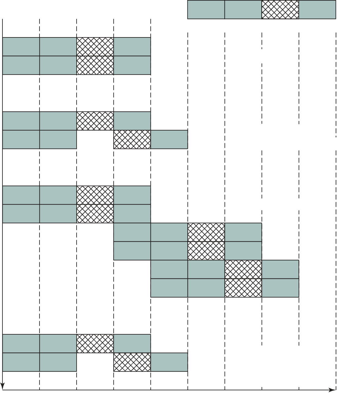
580 CHAPTER 16 / INSTRUCTION-LEVEL PARALLELISM & SUPERSCALAR PROCESSORS
| i0 | Key: | Execute | |
|---|---|---|---|
| Ifetch | Write | ||
| i1 | |||
| i0 | |||
| i1 | |||
| i0 |
|
||
|
|||
| 0 | 1 | 2 | 3 | 4 | 5 | 6 | 7 | 8 | 9 |
|---|
Figure 16.3 illustrates this dependency in a superscalar machine of degree 2. With no dependency, two instructions can be fetched and executed in paral-lel. If there is a data dependency between the first and second instructions, then the second instruction is delayed as many clock cycles as required to remove the dependency. In general, any instruction must be delayed until all of its input values have been produced.
In a simple pipeline, such as illustrated in the upper part of Figure 16.2, the aforementioned sequence of instructions would cause no delay. However, consider the following, in which one of the loads is from memory rather than from a register:
16.2 / DESIgN ISSUES 581
A typical RISC processor takes two or more cycles to perform a load from memory when the load is a cache hit. It can take tens or even hundreds of cycles for a cache miss on all cache levels, because of the delay of an off-chip memory access. One way to compensate for this delay is for the compiler to reorder instructions so that one or more subsequent instructions that do not depend on the memory load can begin flowing through the pipeline. This scheme is less effective in the case of a superscalar pipeline: The independent instructions executed during the load are likely to be executed on the first cycle of the load, leaving the processor with noth-ing to do until the load completes.
In terms of the pipeline, a resource conflict exhibits similar behavior to a data dependency (Figure 16.3). There are some differences, however. For one thing, resource conflicts can be overcome by duplication of resources, whereas a true data depend-ency cannot be eliminated. Also, when an operation takes a long time to complete, resource conflicts can be minimized by pipelining the appropriate functional unit.
16.2 DESIGN ISSUES
582 CHAPTER 16 / INSTRUCTION-LEVEL PARALLELISM & SUPERSCALAR PROCESSORS
The three instructions on the left are independent, and in theory all three could be executed in parallel. In contrast, the three instructions on the right cannot be exe-cuted in parallel because the second instruction uses the result of the first, and the third instruction uses the result of the second.
As was mentioned, machine parallelism is not simply a matter of having multiple instances of each pipeline stage. The processor must also be able to identify instruc-tion-level parallelism and orchestrate the fetching, decoding, and execution of instructions in parallel. [JOHN91] uses the term instruction issue to refer to the process of initiating instruction execution in the processor’s functional units and the term instruction issue policy to refer to the protocol used to issue instructions. In general, we can say that instruction issue occurs when instruction moves from the decode stage of the pipeline to the first execute stage of the pipeline.
In essence, the processor is trying to look ahead of the current point of execu-tion to locate instructions that can be brought into the pipeline and executed. Three types of orderings are important in this regard:
16.2 / DESIgN ISSUES 583
In general terms, we can group superscalar instruction issue policies into the following categories:
Figure 16.4a gives an example of this policy. We assume a superscalar pipeline capable of fetching and decoding two instructions at a time, having three separate functional units (e.g., two integer arithmetic and one floating-point arithmetic), and having two instances of the write-back pipeline stage. The example assumes the following constraints on a six-instruction code fragment:
■ I1 requires two cycles to execute.
In this example, the elapsed time from decoding the first instruction to writing the last results is eight cycles.
in-orderissuewithout-of-ordercompletionOut-of-order completion is used in scalar RISC processors to improve the performance of instructions that require multiple cycles. Figure 16.4b illustrates its use on a superscalar processor. Instruction I2 is allowed to run to completion prior to I1. This allows I3 to be completed earlier, with the net result of a savings of one cycle.
(a) In-order issue and in-order completion
Instruction I2 cannot execute before instruction I1, because it needs the result in register R3 produced in I1; this is an example of a true data dependency, as described in Section 16.1. Similarly, I4 must wait for I3, because it uses a result produced by I3. What about the relationship between I1 and I3? There is no data dependency here, as we have defined it. However, if I3 executes to completion prior to I1, then the wrong value of the contents of R3 will be fetched for the execution of I4. Consequently, I3 must complete after I1 to produce the correct output values. To ensure this, the issuing of the third instruction must be stalled if its result might later be overwritten by an older instruction that takes longer to complete.
Out-of-order completion requires more complex instruction issue logic than in-order completion. In addition, it is more difficult to deal with instruction inter-rupts and exceptions. When an interrupt occurs, instruction execution at the current
To allow out-of-order issue, it is necessary to decouple the decode and execute stages of the pipeline. This is done with a buffer referred to as an instruction win-dow. With this organization, after a processor has finished decoding an instruction, it is placed in the instruction window. As long as this buffer is not full, the processor can continue to fetch and decode new instructions. When a functional unit becomes available in the execute stage, an instruction from the instruction window may be issued to the execute stage. Any instruction may be issued, provided that (1) it needs the particular functional unit that is available, and (2) no conflicts or dependencies block this instruction. Figure 16.5 suggests this organization.
The result of this organization is that the processor has a lookahead capability, allowing it to identify independent instructions that can be brought into the execute stage. Instructions are issued from the instruction window with little regard for their original program order. As before, the only constraint is that the program execution behaves correctly.
| Fetch | Decode | Rename | Dispatch | Issue | Register read | Execute | Write back | Commit |
|---|---|---|---|---|---|---|---|---|
| In-order front end | Out-of-order execution | |||||||
The instruction window is depicted in Figure 16.4c to illustrate its role. How-ever, this window is not an additional pipeline stage. An instruction being in the window simply implies that the processor has sufficient information about that instruction to decide when it can be issued.
The out-of-order issue, out-of-order completion policy is subject to the same constraints described earlier. An instruction cannot be issued if it violates a depend-ency or conflict. The difference is that more instructions are available for issuing, reducing the probability that a pipeline stage will have to stall. In addition, a new dependency, which we referred to earlier as an antidependency (also called write after read [WAR] dependency), arises. The code fragment considered earlier illus-trates this dependency:
One common technique that is used to support out-of-order completion is the reorder buffer. The reorder buffer is temporary storage for results completed out of order that are then committed to the register file in program order. A related con-cept is Tomasulo’s algorithm. Appendix N examines these concepts.
Register Renaming
Antidependencies and output dependencies are both examples of storage con-flicts. Multiple instructions are competing for the use of the same register locations, generating pipeline constraints that retard performance. The problem is made more acute when register optimization techniques are used (as discussed in Chapter 15), because these compiler techniques attempt to maximize the use of registers, hence maximizing the number of storage conflicts.
One method for coping with these types of storage conflicts is based on a traditional resource-conflict solution: duplication of resources. In this context, the technique is referred to as register renaming. In essence, registers are allocated dynamically by the processor hardware, and they are associated with the values needed by instructions at various points in time. When a new register value is cre-ated (i.e., when an instruction executes that has a register as a destination oper-and), a new register is allocated for that value. Subsequent instructions that access that value as a source operand in that register must go through a renaming process: the register references in those instructions must be revised to refer to the register containing the needed value. Thus, the same original register reference in several different instructions may refer to different actual registers, if different values are intended.

Scoreboarding Simulator An alternative to register renaming is a scoreboarding. In essence, scoreboard-ing is a bookkeeping technique that allows instructions to execute whenever they are not dependent on previous instructions and no structural hazards are present. See Appendix N for a discussion.
The two graphs, combined, yield some important conclusions. The first is that it is probably not worthwhile to add functional units without register renaming. There
|
Window size | 8 | 16 | 32 | ||||||||||||||||||||||||||||||||||||||||||||||||||||||||||||||||||||||||||||||||||||||||||||||||||||||||||||||||||||||||||||||||||||||||||||||||||||||||||||||||||||||||||||||||||||||||||||||||||||||||||||||||||||||||||||||||||||||||||||||||||||||||||||||||||||||
|---|---|---|---|---|---|---|---|---|---|---|---|---|---|---|---|---|---|---|---|---|---|---|---|---|---|---|---|---|---|---|---|---|---|---|---|---|---|---|---|---|---|---|---|---|---|---|---|---|---|---|---|---|---|---|---|---|---|---|---|---|---|---|---|---|---|---|---|---|---|---|---|---|---|---|---|---|---|---|---|---|---|---|---|---|---|---|---|---|---|---|---|---|---|---|---|---|---|---|---|---|---|---|---|---|---|---|---|---|---|---|---|---|---|---|---|---|---|---|---|---|---|---|---|---|---|---|---|---|---|---|---|---|---|---|---|---|---|---|---|---|---|---|---|---|---|---|---|---|---|---|---|---|---|---|---|---|---|---|---|---|---|---|---|---|---|---|---|---|---|---|---|---|---|---|---|---|---|---|---|---|---|---|---|---|---|---|---|---|---|---|---|---|---|---|---|---|---|---|---|---|---|---|---|---|---|---|---|---|---|---|---|---|---|---|---|---|---|---|---|---|---|---|---|---|---|---|---|---|---|---|---|---|---|---|---|---|---|---|---|---|---|---|---|---|---|---|---|---|---|---|---|---|---|---|---|---|---|---|---|---|---|---|---|---|---|---|
| (construction) | ||||||||||||||||||||||||||||||||||||||||||||||||||||||||||||||||||||||||||||||||||||||||||||||||||||||||||||||||||||||||||||||||||||||||||||||||||||||||||||||||||||||||||||||||||||||||||||||||||||||||||||||||||||||||||||||||||||||||||||||||||||||||||||||||||||||||||
1 0 |
0 |
|||||||||||||||||||||||||||||||||||||||||||||||||||||||||||||||||||||||||||||||||||||||||||||||||||||||||||||||||||||||||||||||||||||||||||||||||||||||||||||||||||||||||||||||||||||||||||||||||||||||||||||||||||||||||||||||||||||||||||||||||||||||||||||||||||||||||
| base | +ld/st | +alu |
|
base | ||||||||||||||||||||||||||||||||||||||||||||||||||||||||||||||||||||||||||||||||||||||||||||||||||||||||||||||||||||||||||||||||||||||||||||||||||||||||||||||||||||||||||||||||||||||||||||||||||||||||||||||||||||||||||||||||||||||||||||||||||||||||||||||||||||||
16.2 / DESIgN ISSUES 589
is some slight improvement in performance, but at the cost of increased hardware complexity. With register renaming, which eliminates antidependencies and out-put dependencies, noticeable gains are achieved by adding more functional units. Note, however, that there is a significant difference in the amount of gain achievable between using an instruction window of 8 versus a larger instruction window. This indicates that if the instruction window is too small, data dependencies will prevent effective utilization of the extra functional units; the processor must be able to look quite far ahead to find independent instructions to utilize the hardware more fully.
With the advent of RISC machines, the delayed branch strategy was explored. This allows the processor to calculate the result of conditional branch instructions before any unusable instructions have been prefetched. With this method, the pro-cessor always executes the single instruction that immediately follows the branch.
This keeps the pipeline full while the processor fetches a new instruction stream.
590 CHAPTER 16 / INSTRUCTION-LEVEL PARALLELISM & SUPERSCALAR PROCESSORS
Figure 16.7 Conceptual Depiction of Superscalar Processing
The final step mentioned in the preceding paragraph is referred to as commit-ting, or retiring, the instruction. This step is needed for the following reason. Because of the use of parallel, multiple pipelines, instructions may complete in an order dif-ferent from that shown in the static program. Further, the use of branch prediction and speculative execution means that some instructions may complete execution and then must be abandoned because the branch they represent is not taken. Therefore, permanent storage and program-visible registers cannot be updated immediately when instructions complete execution. Results must be held in some sort of tempor-ary storage that is usable by dependent instructions and then made permanent when it is determined that the sequential model would have executed the instruction.
■ Mechanisms for initiating, or issuing, multiple instructions in parallel.
■ Resources for parallel execution of multiple instructions, including multiple pipelined functional units and memory hierarchies capable of simultaneously servicing multiple memory references.
Although the concept of superscalar design is generally associated with the RISC architecture, the same superscalar principles can be applied to a CISC machine. Per-haps the most notable example of this is the Intel x86 architecture. The evolution of superscalar concepts in the Intel line is interesting to note. The 386 is a traditional CISC nonpipelined machine. The 486 introduced the first pipelined x86 processor, reducing the average latency of integer operations from between two and four cycles to one cycle, but still limited to executing a single instruction each cycle, with no superscalar elements. The original Pentium had a modest superscalar component, consisting of the use of two separate integer execution units. The Pentium Pro intro-duced a full-blown superscalar design with out-of-order execution. Subsequent x86 models have refined and enhanced the superscalar design.
Figure 16.8 shows the current version of the x86 pipeline architecture. Intel refers to a pipeline architecture as a microarchitecture. The microarchitecture
| Instruction fetch and predecode |
|---|
| Rename/Allocator |
|---|
L1 data cache and DTLB
1. L1 data cache of the initiating core
2. L1 data cache of other cores and L2 cache
| (a) Cache Parameters | ||||
|---|---|---|---|---|
|
|
|||
|
|
|||
|
|
|||
|
||||
|
||||
|
|
|||
16.3 / INTEL CORE MICROARCHITECTURE 593
■ An in-order retirement unit that ensures the results of execution of micro-ops are processed and architectural states and the processor's register set are updated according to the original program order.
In effect, the Intel Core Microarchitecture implements a CISC instruction set architecture on a RISC microarchitecture. The inner RISC micro-ops pass through a pipeline with at least 14 stages; in some cases, the micro-op requires multiple exe-cution stages, resulting in an even longer pipeline. This contrasts with the five-stage pipeline (Figure 14.21) used on the earlier Intel x86 processors and on the Pentium.
Once the instruction is executed, the history portion of the appropriate entry is updated to reflect the result of the branch instruction. If this instruction is not represented in the BTB, then the address of this instruction is loaded into an entry in the BTB; if necessary, an older entry is deleted.
The description of the preceding two paragraphs fits, in general terms, the branch prediction strategy used on the original Pentium model, as well as the later
■ For IP-relative backward conditional branches, predict taken. This rule reflects the typical behavior of loops.
■ For IP-relative forward conditional branches, predict not taken.
■ Decode all prefixes associated with instructions.
■ Mark various properties of instructions for the decoders (for example, “is branch”).
The resulting micro-op sequence is delivered to the rename/allocator module.
Out-of-Order Execution Logic
■ The allocator allocates one of the 128 integer or floating-point register entries for the result data value of the micro-op, and possibly a load or store buffer used to track one of the 48 loads or 24 stores in the machine pipeline.
■ The allocator allocates an entry in one of the two micro-op queues in front of the instruction schedulers.
■ Alias Register: If the micro-op references one of the 16 architectural registers, this entry redirects that reference to one of the 128 hardware registers.
Micro-ops enter the ROB in order. Micro-ops are then dispatched from the ROB to the Dispatch/Execute unit out of order. The criterion for dispatch is that the appropriate execution unit and all necessary data items required for this microop are available. Finally, micro-ops are retired from the ROB in order. To accomplish in-order retirement, micro-ops are retired oldest first after each micro-op has been designated as ready for retirement.
micro-opqueuing After resource allocation and register renaming, micro-ops are placed in one of two micro-op queues, where they are held until there is room in the schedulers. One of the two queues is for memory operations (loads and stores) and the other for micro-ops that do not involve memory references. Each queue obeys a FIFO (first-in-first-out) discipline, but no order is maintained between queues. That is, a micro-op may be read out of one queue out of order with respect to micro-ops in the other queue. This provides greater flexibility to the schedulers.
micro-opschedulinganddispatching The schedulers are responsible for retrieving micro-ops from the micro-op queues and dispatching these for execution. Each scheduler looks for micro-ops in whose status indicates that the micro-op has all of its operands. If the execution unit needed by that micro-op is available, then the scheduler fetches the micro-op and dispatches it to the appropriate execution unit. Up to six micro-ops can be dispatched in one cycle. If more than one micro-op is available for a given execution unit, then the scheduler dispatches them in sequence from the queue. This is a sort of FIFO discipline that favors in-order execution, but by this time the instruction stream has been so rearranged by dependencies and branches that it is substantially out of order.
16.4 ARM CORTEX-A8
Recent implementations of the ARM architecture have seen the introduction of superscalar techniques in the instruction pipeline. In this section, we focus on the ARM Cortex-A8, which provides a good example of a RISC-based superscalar design.
13-stage integer pipeline

| 5 stages | 6 stages |
|---|
Figure 16.9 Architectural Block Diagram of ARM Cortex-A8
The instruction fetch unit predicts the instruction stream, fetches instructions from the L1 instruction cache, and places the fetched instructions into a buffer for con-sumption by the decode pipeline. The instruction fetch unit also includes the L1
| F0 | F1 | F2 | D0 | D1 | D2 | D3 | D4 |
|---|---|---|---|---|---|---|---|
| Branch |
|
12- | Early | Decode | Replay | Score | Final |
| mispredict | |||||||
| AGU | Dec | ||||||
| + | /seq | board | |||||
| decode | queue | ||||||
| + | decode | ||||||
| read/ | |||||||
|
Early | Decode | issue | ||||
| write | |||||||
| decode | logic |
GHB
mispredict Replay
| INST 0 |
|
E1 | E2 | E3 | E4 | E5 | ALU/ |
|---|---|---|---|---|---|---|---|
| Shift | ALU | SAT | BP | WB | |||
| Architectural register fle | MUL | MUL | MUL | ACC | WB | ||
| pipe 0 | |||||||
| 1 | 2 | 3 | |||||
| INST 1 | Shift | ALU | SAT | BP | WB | ALU | |
| pipe 1 | |||||||
| AGU | Format | L2 | WB | ||||
| forward | update |
(c) Instruction execute and load/store pipeline
Figure 16.10 ARM Cortex-A8 Integer Pipeline
F3: Instruction data are placed into the instruction queue. If an instruction results in branch prediction, the new target address is sent to the address gen-eration unit.
To minimize the branch penalties typically associated with a deeper pipeline, the Cortex-A8 processor implements a two-level global history branch predictor, consisting of the branch target buffer (BTB) and the global history buffer (GHB). These data structures are accessed in parallel with instruction fetches. The BTB indicates whether or not the current fetch address will return a branch instruction and its branch target address. It contains 512 entries. On a hit in the BTB a branch is pre-dicted and the GHB is accessed. The GHB consists of 4096 2-bit counters that encode the strength and direction information of branches. The GHB is indexed by 10-bit his-tory of the direction of the last ten branches encountered and 4 bits of the PC. In add-ition to the dynamic branch predictor, a return stack is used to predict subroutine return addresses. The return stack has eight 32-bit entries that store the link register value in r14 and the ARM or Thumb state of the calling function. When a return-type instruc-tion is predicted taken, the return stack provides the last pushed address and state.
hazards and recovery from flush conditions straightforward. Thus, the main concern of the instruction decode pipeline is the prevention of RAW hazards.
Each instruction goes through five stages of processing.D0: Thumb instructions are decompressed into 32-bit ARM instructions. A preliminary decode function is performed.
In the first two stages, the instruction type, the source and destination oper-ands, and resource requirements for the instruction are determined. A few less commonly used instructions are referred to as multicycle instructions. The D1 stage breaks these instructions down into multiple instruction opcodes that are sequenced individually through the execution pipeline.
The pending queue serves two purposes. First, it prevents a stall signal from D3 from rippling any further up the pipeline. Second, by buffering instructions, there should always be two instructions available for the dual pipeline. In the case where only one instruction is issued, the pending queue enables two instructions to proceed down the pipeline together, even if they were originally sent from the fetch unit in different cycles.
The instruction execute unit consists of two symmetric arithmetic logic unit (ALU) pipelines, an address generator for load and store instructions, and the multiply pipeline.
The execute pipelines also perform register write back. The instruction execute unit:
■ Generates the virtual addresses for loads and stores and the base write-back value, when required.
■ Supplies formatted data for stores and forwards data and flags.
E2: The ALU unit (see Figure 14.25) performs its function.
E3: If needed, this stage completes saturation arithmetic used by some ARM data processing instructions.
|
Description | Example | Cycle | Restriction |
|---|---|---|---|---|
|
LDR r5, [r6] STR r7, [r8] MOV r9, r10 |
|||
|
|
|||
|
|
|||
| Data out- put hazard |
|
|
||
|
|
|||
| Multi-cycle instructions | 4 |
|
E3: In the case of a load, data are returned and formatted for forwarding to the ALU or MUL unit. In the case of a store, the data are formatted and ready to be written into the cache.
E4: Performs updates to the L2 cache, if required.
SIMD and Floating-Point Pipeline
All SIMD and floating-point instructions pass through the integer pipeline and are pro-cessed in a separate 10-stage pipeline (Figure 16.11). This unit, referred to as the NEON unit, handles packed SIMD instructions, and provides two types of floating-point sup-port. If implemented, a vector floating-point (VFP) coprocessor performs floating-point operations in compliance with IEEE 754. If the coprocessor is not present, then sepa-rate multiply and add pipelines implement the floating-point operations.
|
REg | DUP | MUL | MUL | ACC | ACC | WB | Integer | |||
|---|---|---|---|---|---|---|---|---|---|---|---|
| 1 | 2 | 1 | 2 | ||||||||
| Shift 1 | WB | ALU, | |||||||||
| Shift 2 | Shift 3 | MAC, | |||||||||
| Dec | Score- | SHIFT | |||||||||
| FMT | ALU | ABS | WB | pipes | |||||||
| Inst | read | ||||||||||
| queue | board | ||||||||||
| queue | + | ||||||||||
| + | + | ||||||||||
| + | M3 | FDUP | FMUL | FMUL | FMUL | FMUL | WB | Non-IEEE | |||
| Rd/Wr | Issue | ||||||||||
| Inst | fwding | ||||||||||
| check | logic | ||||||||||
| Dec | muxes | ||||||||||
| 1 | 2 | 3 | 4 | FMUL pipe | |||||||
| FFMT | WB | Non-IEEE | |||||||||
| FADD | FADD | FADD | FADD | ||||||||
| 1 | 2 | 3 | 4 | FADD pipe | |||||||
IEEE
■ Processor core: Includes a three-stage pipeline, a register bank, and a memory interface.
■ Memory protection unit: Protects critical data used by the operating system from user applications, separating processing tasks by disallowing access to each other’s data, disabling access to memory regions, allowing memory regions to be defined as read-only, and detecting unexpected memory accesses that could potentially break the system.
16.5 / ARM CORTEx-M3 605
|
Cortex-M3 processor core | ‡ | ||||
|---|---|---|---|---|---|---|
| Fetch | Decode | |||||
| Register bank |
|
|||||
| Memory interface | ||||||
| ‡ |
|
|||||
|
|
|---|
■ Debug access port: Provides an interface for external debug access to the processor.
■ Embedded trace macrocell: Is an application-driven trace source that supports printf() style debugging to trace operating system and application events, and generates diagnostic system information.
■ one word-aligned Thumb-2 instruction, or
606 CHAPTER 16 / INSTRUCTION-LEVEL PARALLELISM & SUPERSCALAR PROCESSORS
This decode stage performs three key functions:
■ Instruction decode and register read: Decodes Thumb and Thumb-2 instructions.
To keep the processor as simple as possible, the Cortex-M3 processor does not use branch prediction, but instead use the simple techniques of branch forwarding and branch speculation, defined as follows:
■ Branch forwarding: The term forwarding refers to presenting an instruction address to be fetched from memory. The processor forwards certain branch types, by which the memory transaction of the branch is presented at least one cycle earlier than when the opcode reaches execute. Branch forwarding increases the performance of the core, because branches are a significant part of embedded controller applications. Branches affected are PC relative with immediate offset, or use link register (LR) as the target register.
16.5 / ARM CORTEx-M3 607
Figure 16.13 clarifies the manner in which branches are handled, which can be described as follows:
Data
| AGU | Address |
|
|---|---|---|
| phase | ||
| and | ||
branch
Multiply
| read | Shift | |
|---|---|---|
Branch
Figure 16.13 ARM Cortex-M3 Pipeline
608 CHAPTER 16 / INSTRUCTION-LEVEL PARALLELISM & SUPERSCALAR PROCESSORS
|
|---|
Review Questions
16.2 |
|
||
|---|---|---|---|
| 0 | ADD | ||
| 1 | LOAD | ||
| 2 | AND | ||
| 3 | ADD |
|
|
| 4 | SRL |
|
|
|
|||||
|---|---|---|---|---|---|
The entries under the four pipeline stages indicate the clock cycle at which each instruction begins each phase. In this program, the second ADD instruction (instruc-tion 3) depends on the LOAD instruction (instruction 1) for one of its operands, r6. Because the LOAD instruction takes five clock cycles, and the issue logic encounters the dependent ADD instruction after two clocks, the issue logic must delay the ADD instruction for three clock cycles. With an out-of-order capability, the processor can stall instruction 3 at clock cycle 4, and then move on to issue the following three inde-pendent instructions, which enter execution at clocks 6, 8, and 9. The LOAD finishes execution at clock 9, and so the dependent ADD can be launched into execution on clock 10.
a. Complete the preceding table.
/R3 d (R7)/
/R8 d Memory (R3)/ /R3 d (R3) + 4/
/R9 d Memory (R3)//Branch if (R9) > (R8)/
16.5 16.6 |
Figure 16.15 shows an example of a superscalar processor organization. The processor can issue two instructions per cycle if there is no resource conflict and no data depen-dence problem. There are essentially two pipelines, with four processing stages (fetch, decode, execute, and store). Each pipeline has its own fetch decode and store unit. Four functional units (multiplier, adder, logic unit, and load unit) are available for use in the execute stage and are shared by the two pipelines on a dynamic basis. The two store units can be dynamically used by the two pipelines, depending on availability at a particular cycle. There is a lookahead window with its own fetch and decoding logic.
|
|---|
b. Show the pipeline activity for this program on the processor of Figure 16.15 using in-order issue with in-order completion policies and using a presentation similar to Figure 16.2.
b. Repeat for in-order issue with out-of-order completion.
| Decode | Execute | Write |
|
||||||||||||||||||||||||||||||||||||||||||||||||
|---|---|---|---|---|---|---|---|---|---|---|---|---|---|---|---|---|---|---|---|---|---|---|---|---|---|---|---|---|---|---|---|---|---|---|---|---|---|---|---|---|---|---|---|---|---|---|---|---|---|---|---|
|
|
||||||||||||||||||||||||||||||||||||||||||||||||||
|
|||||||||||||||||||||||||||||||||||||||||||||||||||
|
|||||||||||||||||||||||||||||||||||||||||||||||||||
16.6 / KEy TERMS, REVIEw QUESTIONS, AND PRObLEMS 611
| f3 | d3 | Load | s2 |
|---|---|---|---|
| Lookahead window | e2 | ||
Figure 16.15 A Dual-Pipeline Superscalar Processor
second level is the branch behavior of the last s occurrences of that unique pattern of the last n branches. For each conditional branch instruction in a program, there is an entry in a Branch History Table (BHT). Each entry consists of n bits corresponding to the last n executions of the branch instruction, with a 1 if the branch was taken and a 0 if the branch was not. Each BHT entry indexes into a Pattern Table (PT) that has 2n entries, one for each possible pattern of n bits. Each PT entry consists of s bits that are used in branch prediction, as was described in Chapter 14 (e.g., Figure 14.19). When a conditional branch is encountered during instruction fetch and decode, the address of the instruction is used to retrieve the appropriate BHT entry, which shows the recent history of the instruction. Then, the BHT entry is used to retrieve the appropriate PT entry for branch prediction. After the branch is executed, the BHT entry is updated, and then the appropriate PT entry is updated.
| From w | ||
|---|---|---|
|
||
|
| T | 0/N | N | N | T | N | N | N | N | 1/N | T | N | N | 0/N | N | |||
|---|---|---|---|---|---|---|---|---|---|---|---|---|---|---|---|---|---|
| T | |||||||||||||||||
| 1/T | 0/N | ||||||||||||||||
| T | |||||||||||||||||
| (a) |
|
2/T | (b) | T | 3/T | 2/T | N | (c) | |||||||||
| T | |||||||||||||||||
| T | T | ||||||||||||||||
|
N | N | |||||||||||||||
| N | N | 0/N | |||||||||||||||
| 0/N | 1/N | ||||||||||||||||
| T | T | ||||||||||||||||
| (d) | (e) |
b. With this algorithm, the prediction is not based on just the recent history of this particular branch instruction. Rather, it is based on the recent history of all pat-terns of branches that match the n-bit pattern in the BHT entry for this instruc-tion. Suggest a rationale for such a strategy.


17.2 Symmetric Multiprocessors
Organization
Multiprocessor Operating System Design Considerations17.3 Cache Coherence and the MESI Protocol Software Solutions
Hardware Solutions
The MESI Protocol17.8 Key Terms, Review Questions, and Problems
613
As computer technology has evolved, and as the cost of computer hard-ware has dropped, computer designers have sought more and more opportunities for parallelism, usually to enhance performance and, in some cases, to increase availability. After an overview, this chapter looks at some of the most prominent approaches to parallel organization. First, we examine symmetric multiproces-sors (SMPs), one of the earliest and still the most common example of paral-lel organization. In an SMP organization, multiple processors share a common memory. This organization raises the issue of cache coherence, to which a sep-arate section is devoted. Next, the chapter examines multithreaded processors and chip multiprocessors. Then we describe clusters, which consist of multiple independent computers organized in a cooperative fashion. Clusters have become increasingly common to support workloads that are beyond the capacity of a single SMP. Another approach to the use of multiple processors that we examine is that of nonuniform memory access (NUMA) machines. The NUMA approach is relatively new and not yet proven in the marketplace, but is often considered as an alternative to the SMP or cluster approach. Finally, this chapter looks at cloud computing architecture.
17.1 / MulTiPlE PRoCEssoR oRgAnizATions 615
■ Single instruction, multiple data (SIMD) stream: A single machine instruction controls the simultaneous execution of a number of processing elements on a lockstep basis. Each processing element has an associated data memory, so that instructions are executed on different sets of data by different processors. Vec-tor and array processors fall into this category, and are discussed in Section 18.7.
■ Multiple instruction, single data (MISD) stream: A sequence of data is trans-mitted to a set of processors, each of which executes a different instruction sequence. This structure is not commercially implemented.
Figure 17.2 illustrates the general organization of the taxonomy of Figure 17.1. Figure 17.2a shows the structure of an SISD. There is some sort of control unit (CU) that provides an instruction stream (IS) to a processing unit (PU). The processing
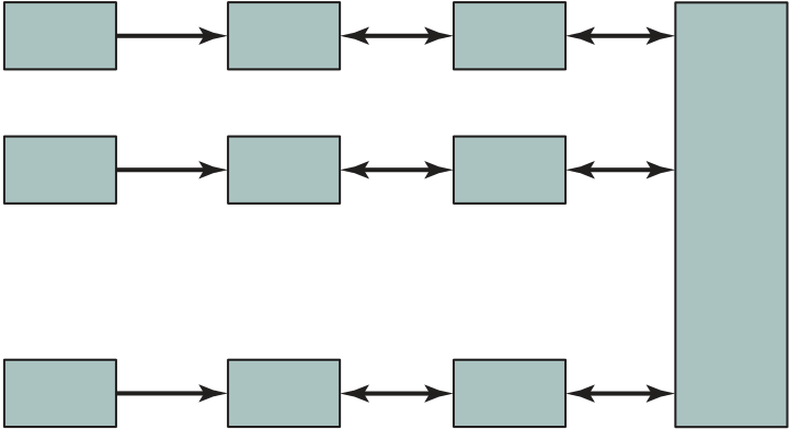
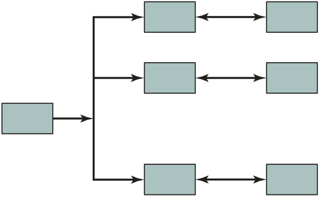
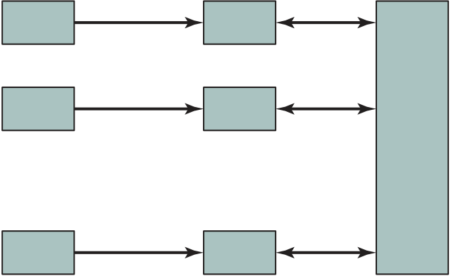
| Single instruction, | Multiple instruction, |
|
|||
|---|---|---|---|---|---|
|
multiple data stream | single data stream | |||
| (SISD) | (SIMD) | (MISD) | (MIMD) | ||
| Uniprocessor | Vector | Array |  |
||
| Shared memory | |||||
| processor | (tightly coupled) | ||||
Clusters
| CU | IS | PU | DS | PU1 | DS | LM1 | ||||||
|---|---|---|---|---|---|---|---|---|---|---|---|---|
| (a) SISD | PU2 | DS | LM2 | |||||||||
| CU1 | IS | PU1 |
|
CU | IS | • | ||||||
| • | ||||||||||||
| • | ||||||||||||
| PUn | DS | LMn | ||||||||||
| CU2 | IS | PU2 | DS | Shared memory |
|
|||||||
| • | CU1 | IS | PU1 | DS | ||||||||
| • | ||||||||||||
| • | ||||||||||||
| CUn | IS | PUn | CU2 | IS | PU2 | DS | ||||||
| • | ||||||||||||
|
SISD=Single instruction, =single data stream SIMD=Single instruction, multiple data stream MIMD=Multiple instruction, multiple data stream | • | ||||||||||
| • | ||||||||||||
| CUn | IS | PUn | DS |
|
||||||||
The design issues relating to SMPs, clusters, and NUMAs are complex, involv-ing issues relating to physical organization, interconnection structures, interprocessor communication, operating system design, and application software techniques. Our concern here is primarily with organization, although we touch briefly on operating system design issues.
17.2 SYMMETRIC MULTIPROCESSORS
4. All processors can perform the same functions (hence the term symmetric).
5. The system is controlled by an integrated operating system that provides interaction between processors and their programs at the job, task, file, and data element levels.
Process 1 Process 2 |
Time | ||||
|---|---|---|---|---|---|
Process 2 Process 3 |
|---|
■ Availability: In a symmetric multiprocessor, because all processors can per-form the same functions, the failure of a single processor does not halt the machine. Instead, the system can continue to function at reduced performance.
■ Incremental growth: A user can enhance the performance of a system by add- ing an additional processor.
Figure 17.4 depicts in general terms the organization of a multiprocessor system. There are two or more processors. Each processor is self- contained, including a con-trol unit, ALU, registers, and, typically, one or more levels of cache. Each processor has access to a shared main memory and the I/O devices through some form of inter-connection mechanism. The processors can communicate with each other through memory (messages and status information left in common data areas). It may also be possible for processors to exchange signals directly. The memory is often organized
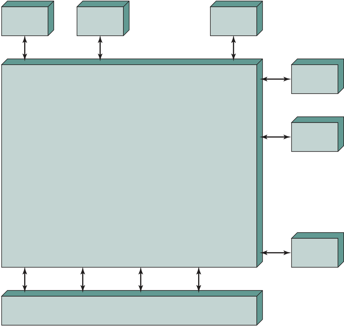
| Processor | Processor | • • • |
|---|
Interconnection
The most common organization for personal computers, workstations, and servers is the time- shared bus. The time- shared bus is the simplest mechanism for constructing a multiprocessor system (Figure 17.5). The structure and interfaces are basically the same as for a single- processor system that uses a bus interconnection. The bus consists of control, address, and data lines. To facilitate DMA transfers from I/O subsystems to processors, the following features are provided:
■ Addressing: It must be possible to distinguish modules on the bus to deter- mine the source and destination of data.
620 CHAPTER 17 / PARAllEl PRoCEssing
|
Processor | • • • | Processor |
|---|---|---|---|
| L1 cache | L1 cache | L1 cache | |
| L2 cache | L2 cache |
Figure 17.5 Symmetric Multiprocessor Organization
The bus organization has several attractive features:
The use of caches introduces some new design considerations. Because each local cache contains an image of a portion of memory, if a word is altered in one
17.3 / CACHE CoHEREnCE And THE MEsi PRoToCol 621
■ Scheduling: Any processor may perform scheduling, so conflicts must be avoided. The scheduler must assign ready processes to available processors.
■ Synchronization: With multiple active processes having potential access to shared address spaces or shared I/O resources, care must be taken to provide effective synchronization. Synchronization is a facility that enforces mutual exclusion and event ordering.
622 CHAPTER 17 / PARAllEl PRoCEssing
problem. The essence of the problem is this: Multiple copies of the same data can exist in different caches simultaneously, and if processors are allowed to update their own copies freely, an inconsistent view of memory can result. In Chapter 4 we defined two common write policies:
For any cache coherence protocol, the objective is to let recently used local variables get into the appropriate cache and stay there through numerous reads and write, while using the protocol to maintain consistency of shared variables that might be in multiple caches at the same time. Cache coherence approaches have generally been divided into software and hardware approaches. Some implementa-tions adopt a strategy that involves both software and hardware elements. Never-theless, the classification into software and hardware approaches is still instructive and is commonly used in surveying cache coherence strategies.
Software Solutions
More efficient approaches analyze the code to determine safe periods for shared variables. The compiler then inserts instructions into the generated code to enforce cache coherence during the critical periods. A number of techniques have been developed for performing the analysis and for enforcing the results; see [LILJ93] and [STEN90] for surveys.
Hardware Solutions
Directory schemes suffer from the drawbacks of a central bottleneck and the overhead of communication between the various cache controllers and the central controller. However, they are effective in large- scale systems that involve multiple buses or some other complex interconnection scheme.
snoopyprotocols Snoopy protocols distribute the responsibility for maintaining cache coherence among all of the cache controllers in a multipro- cessor. A cache must recognize when a line that it holds is shared with other
With a write- update protocol, there can be multiple writers as well as multiple readers. When a processor wishes to update a shared line, the word to be updated is distributed to all others, and caches containing that line can update it.
Neither of these two approaches is superior to the other under all circum-stances. Performance depends on the number of local caches and the pattern of memory reads and writes. Some systems implement adaptive protocols that employ both write- invalidate and write- update mechanisms.
■ Exclusive: The line in the cache is the same as that in main memory and is not present in any other cache.
■ Shared: The line in the cache is the same as that in main memory and may be present in another cache.
|
|
|||
|---|---|---|---|---|
| Yes | Yes | Yes | No | |
| out of date | valid | valid | — | |
| Copies exist in other caches? | No | No | Maybe | Maybe |
|
|
SHR
Figure 17.6 MESI State Transition Diagram
626 CHAPTER 17 / PARAllEl PRoCEssing
■ If one other cache has a modified copy of the line, then that cache blocks the memory read and provides the line to the requesting cache over the shared bus. The responding cache then changes its line from modified to shared.1 The line sent to the requesting cache is also received and processed by the memory controller, which stores the block in memory.
■ If no other cache has a copy of the line (clean or modified), then no signals are returned. The initiating processor reads the line and transitions the line in its cache from invalid to exclusive.
17.3 / CACHE CoHEREnCE And THE MEsi PRoToCol 627
line back to main memory, and transitions the state of the cache line to invalid (because the initiating processor is going to modify this line). Subsequently, the initiating processor will again issue a signal to the bus of RWITM and then read the line from main memory, modify the line in the cache, and mark the line in the modified state.
■ Modified: The processor already has exclusive control of this line and has the line marked as modified, and so it simply performs the update.
l1-l2 cacheconsistency We have so far described cache coherency protocols in terms of the cooperate activity among caches connected to the same bus or other SMP interconnection facility. Typically, these caches are L2 caches, and each processor also has an L1 cache that does not connect directly to the bus and that therefore cannot engage in a snoopy protocol. Thus, some scheme is needed to maintain data integrity across both levels of cache and across all caches in the SMP configuration.
The most important measure of performance for a processor is the rate at which it executes instructions. This can be expressed as
MIPS rate = f * IPC
The concept of thread used in discussing multithreaded processors may or may not be the same as the concept of software threads in a multiprogrammed operating system. It will be useful to define terms briefly:
■ Process: An instance of a program running on a computer. A process embod- ies two key characteristics:
■ Thread: A dispatchable unit of work within a process. It includes a processor context (which includes the program counter and stack pointer) and its own data area for a stack (to enable subroutine branching). A thread executes sequen-tially and is interruptible so that the processor can turn to another thread.
■ Thread switch: The act of switching processor control from one thread to another within the same process. Typically, this type of switch is much less costly than a process switch.
Broadly speaking, there are four principal approaches to multithreading:
■ Interleaved multithreading: This is also known as fine- grained multithread-ing. The processor deals with two or more thread contexts at a time, switching from one thread to another at each clock cycle. If a thread is blocked because
■ Simultaneous multithreading (SMT): Instructions are simultaneously issued from multiple threads to the execution units of a superscalar processor. This combines the wide superscalar instruction issue capability with the use of multiple thread contexts.
■ Chip multiprocessing: In this case, multiple cores are implemented on a single chip and each core handles separate threads. The advantage of this approach is that the available logic area on a chip is used effectively without depending on ever- increasing complexity in pipeline design. This is referred to as multi-core; we examine this topic separately in Chapter 18.
■ Interleaved multithreaded scalar: This is the easiest multithreading approach to implement. By switching from one thread to another at each clock cycle, the pipeline stages can be kept fully occupied, or close to fully occupied. The hardware must be capable of switching from one thread context to another between cycles.
3Issue slots are the position from which instructions can be issued in a given clock cycle. Recall from Chapter 16 that instruction issue is the process of initiating instruction execution in the processor’s func-tional units. This occurs when an instruction moves from the decode stage of the pipeline to the first execute stage of the pipeline.
| A | A | A | A |
|
||||||||||||||||||||||||||||||||||||||||||||||||
|---|---|---|---|---|---|---|---|---|---|---|---|---|---|---|---|---|---|---|---|---|---|---|---|---|---|---|---|---|---|---|---|---|---|---|---|---|---|---|---|---|---|---|---|---|---|---|---|---|---|---|---|---|
| Cycles |
|
|
||||||||||||||||||||||||||||||||||||||||||||||||||
|
||||||||||||||||||||||||||||||||||||||||||||||||||||
|
||||||||||||||||||||||||||||||||||||||||||||||||||||
| (a) Single-threaded | (b) Interleaved | (c) Blocked | ||||||||||||||||||||||||||||||||||||||||||||||||||
| scalar | multithreading | multithreading | ||||||||||||||||||||||||||||||||||||||||||||||||||
| scalar | scalar | |||||||||||||||||||||||||||||||||||||||||||||||||||
| A | A | A | A | |||||||||||||||||||||||||||||||||||||||||||||||||
|
A | A |
|
|||||||||||||||||||||||||||||||||||||||||||||||||
| A | A | |||||||||||||||||||||||||||||||||||||||||||||||||||
| B | B | |||||||||||||||||||||||||||||||||||||||||||||||||||
| B | ||||||||||||||||||||||||||||||||||||||||||||||||||||
| C | ||||||||||||||||||||||||||||||||||||||||||||||||||||
In the case of interleaved multithreading, it is assumed that there are no control or data dependencies between threads, which simplifies the pipeline design and there-fore should allow a thread switch with no delay. However, depending on the specific design and implementation, block multithreading may require a clock cycle to per-form a thread switch, as illustrated in Figure 17.7. This is true if a fetched instruction triggers the thread switch and must be discarded from the pipeline [UNGE03].
Although interleaved multithreading appears to offer better processor uti-lization than blocked multithreading, it does so at the sacrifice of single- thread performance. The multiple threads compete for cache resources, which raises the probability of a cache miss for a given thread.
■ Very long instruction word (VLIW): A VLIW architecture, such as IA- 64, places multiple instructions in a single word. Typically, a VLIW is constructed by the compiler, which places operations that may be executed in parallel in the same word. In a simple VLIW machine (Figure 17.7g), if it is not possible to com-pletely fill the word with instructions to be issued in parallel, no- ops are used.
■ Interleaved multithreading VLIW: This approach should provide similar efficiencies to those provided by interleaved multithreading on a superscalar architecture.
threads are active, it should usually be possible to issue the maximum number of instructions on each cycle, providing a high level of efficiency.
■ Chip multiprocessor (multicore): Figure 17.7k shows a chip containing four cores, each of which has a two- issue superscalar processor. Each core is assigned a thread, from which it can issue up to two instructions per cycle. We discuss multicore computers in Chapter 18.
■ Absolute scalability: It is possible to create large clusters that far surpass the power of even the largest standalone machines. A cluster can have tens, hun-dreds, or even thousands of machines, each of which is a multiprocessor.
■ Incremental scalability: A cluster is configured in such a way that it is possible to add new systems to the cluster in small increments. Thus, a user can start out with a modest system and expand it as needs grow, without having to go through a major upgrade in which an existing small system is replaced with a larger system.
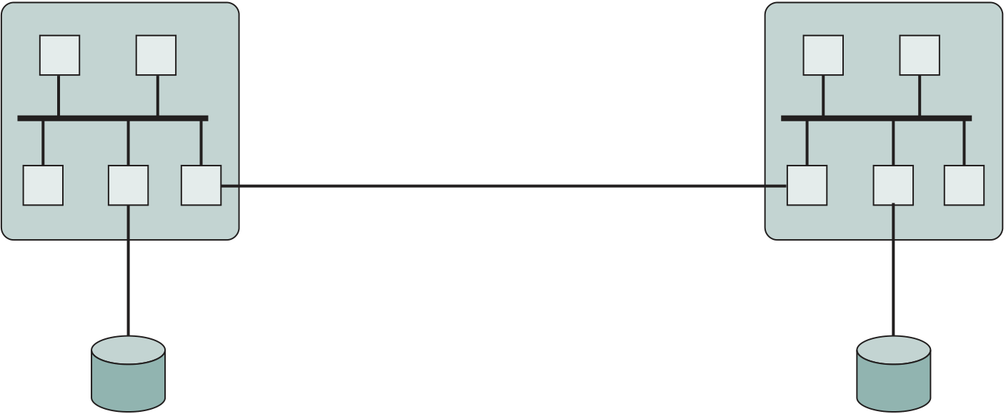
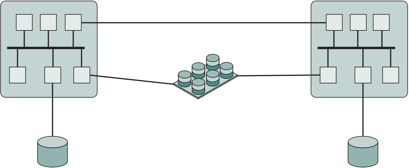
634 CHAPTER 17 / PARAllEl PRoCEssing
| P | I/O | P | High-speed message link | P | I/O | P | M | |
|---|---|---|---|---|---|---|---|---|
| M | I/O |
In the simple classification depicted in Figure 17.8, the other alternative is a shared- disk cluster. In this case, there generally is still a message link between nodes. In addition, there is a disk subsystem that is directly linked to multiple com-puters within the cluster. In this figure, the common disk subsystem is a RAID sys-tem. The use of RAID or some similar redundant disk technology is common in clusters so that the high availability achieved by the presence of multiple computers is not compromised by a shared disk that is a single point of failure.
A clearer picture of the range of cluster options can be gained by looking at functional alternatives. Table 17.2 provides a useful classification along functional lines, which we now discuss.
| Description | Benefits | Limitations | |
|---|---|---|---|
|
|
||
|
|||
|
|||
|
|
||
| Servers Share Disks |
A common, older method, known as passive standby, is simply to have one computer handle all of the processing load while the other computer remains inactive, standing by to take over in the event of a failure of the primary. To coord-inate the machines, the active, or primary, system periodically sends a “heartbeat” message to the standby machine. Should these messages stop arriving, the standby assumes that the primary server has failed and puts itself into operation. This approach increases availability but does not improve performance. Further, if the only information that is exchanged between the two systems is a heartbeat message, and if the two systems do not share common disks, then the standby provides a functional backup but has no access to the databases managed by the primary.
The passive standby is generally not referred to as a cluster. The term cluster is reserved for multiple interconnected computers that are all actively doing pro-cessing while maintaining the image of a single system to the outside world. The term active secondary is often used in referring to this configuration. Three classifi-cations of clustering can be identified: separate servers, shared nothing, and shared memory.
It is also possible to have multiple computers share the same disks at the same time (called the shared disk approach), so that each computer has access to all of the volumes on all of the disks. This approach requires the use of some type of locking facility to ensure that data can only be accessed by one computer at a time.
Operating System Design Issues
loadbalancing A cluster requires an effective capability for balancing the load among available computers. This includes the requirement that the cluster be incrementally scalable. When a new computer is added to the cluster, the load- balancing facility should automatically include this computer in scheduling applications. Middleware mechanisms need to recognize that services can appear on different members of the cluster and may migrate from one member to another.
parallelizingcomputation In some cases, effective use of a cluster requires executing software from a single application in parallel. [KAPP00] lists three general approaches to the problem:
■ Parametric computing: This approach can be used if the essence of the appli-cation is an algorithm or program that must be executed a large number of times, each time with a different set of starting conditions or parameters. A good example is a simulation model, which will run a large number of differ-ent scenarios and then develop statistical summaries of the results. For this approach to be effective, parametric processing tools are needed to organize, run, and manage the jobs in an effective manner.
Cluster Computer Architecture
| PC/workstation | PC/workstation | PC/workstation | PC/workstation | |
|---|---|---|---|---|
|
Comm SW | Comm SW | Comm SW | Comm SW |
|
Net. interface HW | Net. interface HW | Net. interface HW | Net. interface HW |
■ Single entry point: A user logs onto the cluster rather than to an individual computer.
■ Single file hierarchy: The user sees a single hierarchy of file directories under the same root directory.
■ Single user interface: A common graphic interface supports all users, regard- less of the workstation from which they enter the cluster.
■ Single I/O space: Any node can remotely access any I/O peripheral or disk device without knowledge of its physical location.
The remaining items are concerned with providing a single system image.
Returning to Figure 17.9, a cluster will also include software tools for enabling the efficient execution of programs that are capable of parallel execution.Blade Servers
Additional blade
server racks
N 100GbE
|
Eth switch | Eth switch | Eth switch |
|---|---|---|---|
|
The main strength of the SMP approach is that an SMP is easier to manage and configure than a cluster. The SMP is much closer to the original single- processor model for which nearly all applications are written. The principal change required in going from a uniprocessor to an SMP is to the scheduler function. Another ben-efit of the SMP is that it usually takes up less physical space and draws less power than a comparable cluster. A final important benefit is that the SMP products are well established and stable.
Over the long run, however, the advantages of the cluster approach are likely to result in clusters dominating the high- performance server market. Clusters are far superior to SMPs in terms of incremental and absolute scalability. Clusters are also superior in terms of availability, because all components of the system can readily be made highly redundant.
■ Uniform memory access (UMA): All processors have access to all parts of main memory using loads and stores. The memory access time of a processor to all regions of memory is the same. The access times experienced by different processors are the same. The SMP organization discussed in Sections 17.2 and 17.3 is UMA.
■ Nonuniform memory access (NUMA): All processors have access to all parts of main memory using loads and stores. The memory access time of a proces-sor differs depending on which region of main memory is accessed. The last statement is true for all processors; however, for different processors, which memory regions are slower and which are faster differ.
The processor limit in an SMP is one of the driving motivations behind the development of cluster systems. However, with a cluster, each node has its own private main memory; applications do not see a large global memory. In effect, coherency is maintained in software rather than hardware. This memory granularity affects performance and, to achieve maximum performance, software must be tai-lored to this environment. One approach to achieving large- scale multiprocessing while retaining the flavor of SMP is NUMA.
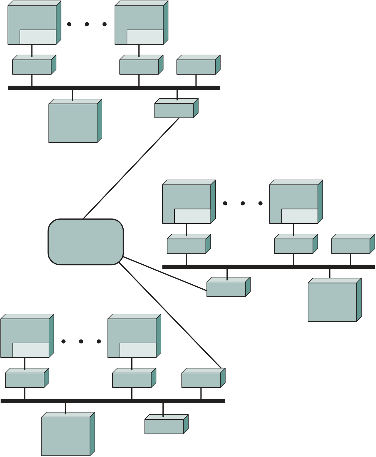
| Interconnect | Processor | Processor | Directory | |
|---|---|---|---|---|
| 2-1 | 2-m | |||
| L1 Cache | L1 Cache | |||
| Network | L2 Cache | L2 Cache | ||
Memory 2
memory N
Figure 17.11 CC- NUMA Organization
1. P2-3 issues a read request on the snoopy bus of node 2 for location 798.
2. The directory on node 2 sees the request and recognizes that the location is in node 1.
7. The value is transferred back to node 2’s directory.
8. Node 2’s directory places the data back on node 2’s bus, acting as a surrogate for the memory that originally held it.
NUMA Pros and Cons
The main advantage of a CC- NUMA system is that it can deliver effective perfor-mance at higher levels of parallelism than SMP, without requiring major software changes. With multiple NUMA nodes, the bus traffic on any individual node is lim-ited to a demand that the bus can handle. However, if many of the memory accesses are to remote nodes, performance begins to break down. There is reason to believe that this performance breakdown can be avoided. First, the use of L1 and L2 caches is designed to minimize all memory accesses, including remote ones. If much of the software has good temporal locality, then remote memory accesses should not be excessive. Second, if the software has good spatial locality, and if virtual memory is in use, then the data needed for an application will reside on a limited num-ber of frequently used pages that can be initially loaded into the memory local to the running application. The Sequent designers report that such spatial locality does appear in representative applications [LOVE96]. Finally, the virtual memory scheme can be enhanced by including in the operating system a page migration mechanism that will move a virtual memory page to a node that is frequently using it; the Silicon Graphics designers report success with this approach [WHIT97].
 |
|---|
Cloud computing was introduced in Chapter 1, where the three service models were discussed. Here we go into greater detail.
Cloud Computing Elements
■ Broad network access: Capabilities are available over the network and accessed through standard mechanisms that promote use by heterogeneous thin or thick client platforms (e.g., mobile phones, laptops, and tablets) as well as other traditional or cloud- based software services.
■ Rapid elasticity: Cloud computing gives you the ability to expand and reduce resources according to your specific service requirement. For example, you may need a large number of server resources for the duration of a specific task. You can then release these resources upon completion of the task.
| ial |
|
|
||||||
| elasticity | service | self-service | ||||||
| Essent | character | |||||||
NIST defines three service models, which can be viewed as nested service alternatives (Figure 17.13). These were defined in Chapter 1, and can be briefly summarized as follows:
■ Software as a service (SaaS): Provides service to customers in the form of soft- ware, specifically application software, running on and accessible in the cloud.
| Cloud application software |
|---|
| (visible only to provider) |
|---|
| to provider) |
|---|
| (developed by subscriber) |
|---|
| (visible to subscriber) |
|---|
| infrastructure |
|---|
| to provider) |
|---|
|
|---|
■ Infrastructure as a service (IaaS): Provides the customer access to the under- lying cloud infrastructure.
NIST defines four deployment models:
Figure 17.14 illustrates the typical cloud service context. An enterprise main-tains workstations within an enterprise LAN or set of LANs, which are connected by a router through a network or the Internet to the cloud service provider. The cloud ser-vice provider maintains a massive collection of servers, which it manages with a variety
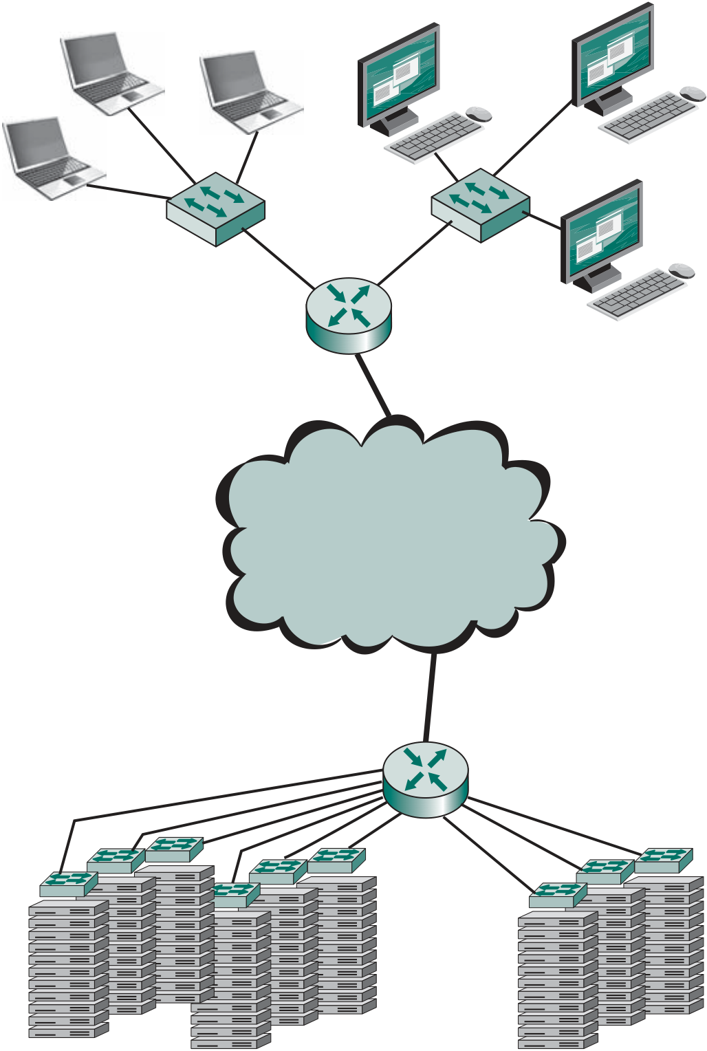
Network
or Internet
Router
Figure 17.14 Cloud Computing Context
of network management, redundancy, and security tools. In the figure, the cloud infra-structure is shown as a collection of blade servers, which is a common architecture.
648 CHAPTER 17 / PARAllEl PRoCEssing
NIST developed the reference architecture with the following objectives in mind:
■ Cloud consumer: A person or organization that maintains a business relation- ship with, and uses service from, cloud providers.
■ Cloud provider (CP): A person, organization, or entity responsible for making a service available to interested parties.
| Cloud | Cloud provider | Cloud | |||
|---|---|---|---|---|---|
| Service orchestration | Cloud | ||||
| consumer | broker | ||||
|
|||||
| Service | |||||
| Cloud | PaaS | Business |
|
acy | intermediation |
| auditor | IaaS | support | Service | ||
| Security | Priv | aggregation | |||
| audit | |||||
| Privacy | Service | ||||
| arbitrage | |||||
| impact audit | |||||
|
|
||||
| Performance | |||||
| audit | |||||
For IaaS, the CP acquires the physical computing resources underlying the service, including the servers, networks, storage, and hosting infrastructure. The IaaS cloud consumer in turn uses these computing resources, such as a virtual com-puter, for their fundamental computing needs.
The cloud carrier is a networking facility that provides connectivity and transport of cloud services between cloud consumers and CPs. Typically, a CP will set up service level agreements (SLAs) with a cloud carrier to provide services consistent with the level of SLAs offered to cloud consumers, and may require the cloud carrier to provide dedicated and secure connections between cloud consum-ers and CPs.
A cloud auditor can evaluate the services provided by a CP in terms of secur-ity controls, privacy impact, performance, and so on. The auditor is an independent entity that can assure that the CP conforms to a set of standards.
650 CHAPTER 17 / PARAllEl PRoCEssing
|
|---|
Review Questions
17.5 What is the difference between software and hardware cache coherent schemes?
17.6 What is the meaning of each of the four states in the MESI protocol?
Problems
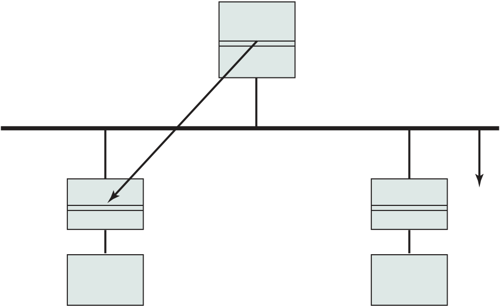
17.7 |
|
|---|
| R( j) | R(i) | W(i) | R( j) |
|
R(i) | Shared | R(i) | ||
|---|---|---|---|---|---|---|---|---|---|
|
|||||||||
| Valid | W(i) | Z( j) | |||||||
| Z( j) | W( j) | Z(i) | R( j) | ||||||
| Z( j) | W( j) |
|
|
||||||
| R( j) | |||||||||
| Z(i) | |||||||||
R(i)
W(i) Z( j) Figure 17.17 Two Cache Coherence Protocolsare used, and the access penalty when all three caches are used. Note the amount of improvement in each case and state your opinion on the value of the L3 cache.
| Memory Subsystem |
|
Cache Size | Hit Rate (%) |
|---|---|---|---|
| L1 cache | 1 | 32 KB | 89 |
| L2 cache | 5 | 256 KB | 5 |
| L3 cache | 14 | 2 MB | 3 |
| Memory | 32 | 8 GB | 3 |


| (a) | (b) | (c) | (d) | ||||||||||||||||||||||||||||||||||||||||||||||||||||||||||||||||||||||||||||||||||||||||||||||||||||
b. Assume that the two threads are to be executed in parallel on a chip multipro-cessor, with each of the two cores on the chip using a simple pipeline. Show an instruction issue diagram similar to Figure 17.7k. Also show a pipeline execution diagram in the style of Figure 17.19.
c. Assume a two- issue superscalar architecture. Repeat part (b) for an interleaved multithreading superscalar implementation, assuming no data dependencies.
d. Repeat part (c) for a blocked multithreading superscalar implementation. e. Repeat for a four- issue SMT architecture.
17.12 |
|
|---|
version is to be executed on a 32-computer cluster.
L5: 10 CONTINUE
Suppose lines 2 and 4 each take two machine cycle times, including all processor and memory- access activities. Ignore the overhead caused by the software loop control statements (lines 1, 3, 5) and all other system overhead and resource conflicts. a. What is the total execution time (in machine cycle times) of the program on a single computer?
|
DOALL K = 1, M DO 10 I = L( K- 1)+1, KL A(I) = B(I)+C(I) 10 CONTINUE SUM(K) = 0 DO 20 J = 1, L SUM(K) = SUM(K) + A(L( K- 1)+J) 20 CONTINUE ENDALL |
|---|
a. The program on the left executes on a uniprocessor. Suppose each line of code L2, L4, and L6 takes one processor clock cycle to execute. For simplicity, ignore the time required for the other lines of code. Initially all arrays are already loaded in main memory and the short program fragment is in the instruction cache. How many clock cycles are required to execute this program?
17.8 / KEy TERMs, REviEw QuEsTions, And PRoblEMs 655
Multicore coMputers
18.1 Hardware Performance Issues
Increase in Parallelism and Complexity Power Consumption18.6 ARM Cortex- A15 MPCore
Interrupt Handling
Cache Coherency
L2 Cache Coherency18.7 IBM zEnterprise EC12 Mainframe
Organization
Cache Structure
This chapter provides an overview of multicore systems. We begin with a look at the hardware performance factors that led to the development of multicore com-puters and the software challenges of exploiting the power of a multicore system. Next, we look at multicore organization. Finally, we examine three examples of multicore products, covering personal computer and workstation systems (Intel), embedded systems (ARM), and mainframes (IBM).
18.1 HARDWARE PERFORMANCE ISSUES
■ Superscalar: Multiple pipelines are constructed by replicating execution resources. This enables parallel execution of instructions in parallel pipelines, so long as hazards are avoided.
| PC 1 | Instruction fetch unit | PC n | Register 1 | Registers n |
|---|---|---|---|---|
| L1 instruction cache |
|
|||
L2 cache
(c) Multicore
Figure 18.1 Alternative Chip Organizations
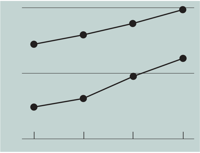
18.1 / Hardware Performance Issues 659
To maintain the trend of higher performance as the number of transistors per chip rises, designers have resorted to more elaborate processor designs (pipelining, super-scalar, SMT) and to high clock frequencies. Unfortunately, power requirements have grown exponentially as chip density and clock frequency have risen. This was shown in Figure 2.2.
One way to control power density is to use more of the chip area for cache memory. Memory transistors are smaller and have a power density an order of magnitude lower than that of logic (see Figure 18.2). As chip transistor density has increased, the percentage of chip area devoted to memory has grown, and is now often half the chip area. Even so, there is still a considerable amount of chip area devoted to processing logic.
Memory
| 1 |
|
0.18 | 0.13 |
|---|
How to use all those logic transistors is a key design issue. As discussed earlier in this section, there are limits to the effective use of such techniques as superscalar and SMT. In general terms, the experience of recent decades has been encapsu-lated in a rule of thumb known as Pollack’s rule [POLL99], which states that per-formance increase is roughly proportional to square root of increase in complexity. In other words, if you double the logic in a processor core, then it delivers only 40% more performance. In principle, the use of multiple cores has the potential to provide near- linear performance improvement with the increase in the number of cores— but only for software that can take advantage.
Power considerations provide another motive for moving toward a mul-ticore organization. Because the chip has such a huge amount of cache memory, it becomes unlikely that any one thread of execution can effectively use all that memory. Even with SMT, multithreading is done in a relatively limited fashion and cannot therefore fully exploit a gigantic cache, whereas a number of relatively inde-pendent threads or processes has a greater opportunity to take full advantage of the cache memory.
Speedup =
time to execute program on a single processor time to execute program onNparallel processors
| 8 | 0% |
|---|
2%
| 0 | 1 | 2 | 3 | 4 | 5 | 6 | 7 |
|---|
Number of processors
(a) Speedup with 0%, 2%, 5%, and 10% sequential portions
| 0 | 1 | 2 | 3 | 4 | 5 | 6 | 7 |
|---|
Figure 18.3 Performance Effect of Multiple Cores
coherence overhead. This overhead results in a curve where performance peaks and then begins to degrade because of the increased burden of the overhead of using multiple processors (e.g., coordination and OS management). Figure 18.3b, from [MCDO05], is a representative example.
[MCDO06] lists the following examples:
■ Multithreaded native applications ( thread- level parallelism): Multithreaded applications are characterized by having a small number of highly threaded processes.
18.2 / sofTware Performance Issues 663
Before turning to an example, we elaborate on the topic of thread- level par-allelism by introducing the concept of threading granularity, which can be defined as the minimal unit of work that can be beneficially parallelized. In general, the finer the granularity the system enables, the less constrained is the programmer in parallelizing a program. Consequently, finer grain threading systems allow paralleli-zation in more situations than coarse- grained ones. The choice of the target gran-ularity of an architecture involves an inherent tradeoff. On the one hand, the finer grain systems are preferable because of the flexibility they afford to the program-mer. On the other hand, the finer the threading granularity, the more significant part of the execution is taken by the threading system overhead.
■ Coarse- grained threading: Individual modules, called systems, are assigned to individual processors. In the Source engine case, this means putting rendering on one processor, AI (artificial intelligence) on another, physics on another, and so on. This is straightforward. In essence, each major module is single threaded and the principal coordination involves synchronizing all the threads with a timeline thread.
■ Fine- grained threading: Many similar or identical tasks are spread across multiple processors. For example, a loop that iterates over an array of data can be split up into a number of smaller parallel loops in individual threads that can be scheduled in parallel.
664 cHaPTer 18 / mulTIcore comPuTers
its own set of data. Other modules, such as scene rendering, can be organized into a number of threads so that the module can execute on a single processor but achieve greater performance as it is spread out over more and more processors.
■ Compute character bone transformations for all characters in all scenes in parallel.
■ Allow multiple threads to draw in parallel.
| Skybox | Main view | Monitor | Etc. |
|---|
Sim and draw
Character
18.3 / mulTIcore organIzaTIon 665
The designers found that simply locking key databases, such as the world list, for a thread was too inefficient. Over 95% of the time, a thread is trying to read from a data set, and only 5% of the time at most is spent in writing to a data set. Thus, a concurrency mechanism known as the single- writer- multiple- readers model works effectively.
■ How cache memory is shared among cores
■ Whether simultaneous multithreading (SMT) is employed
The organization of Figure 18.6b is also one in which there is no on- chip cache sharing. In this, there is enough area available on the chip to allow for L2 cache. An example of this organization is the AMD Opteron. Figure 18.6c shows a similar allocation of chip space to memory, but with the use of a shared L2 cache. The Intel Core Duo has this organization. Finally, as the amount of cache memory available on the chip continues to grow, performance considerations dictate splitting off a separate, shared L3 cache (Figure 18.6d), with dedicated L1 and L2 caches for each core processor. The Intel Core i7 is an example of this organization.
The use of a shared higher- level cache on the chip has several advantages over exclusive reliance on dedicated caches:
Figure 18.6 Multicore Organization Alternatives
3. With proper line replacement algorithms, the amount of shared cache allo-cated to each core is dynamic, so that threads that have less locality (larger working sets) can employ more cache.
18.4 / HeTerogeneous mulTIcore organIzaTIon 667
Simultaneous Multithreading
2. Increase the number of levels of cache memory.
3. Change the length (increase or decrease) and functional components of the instruction pipeline.
The approach that has received the most industry attention is the use of cores that have distinct ISAs. Typically, this involves mixing conventional cores, referred to in this context as CPUs, with specialized cores optimized for certain types of data or applications. Most often, the additional cores are optimized to deal with vector and matrix data processing.
cpu/gpumulticore The most prominent trend in terms of heterogeneous multicore design is the use of both CPUs and graphics processing units (GPUs) on the same chip. GPUs are discussed in detail in the following chapter. Briefly, GPUs are characterized by the ability to support thousands of parallel execution threads. Thus, GPUs are well matched to applications that process large amounts
Figure 18.7 is a typical multicore processor organization. Multiple CPUs and GPUs share on- chip resources, such as the last- level cache (LLC), interconnection network, and memory controllers. Most critical is the way in which cache manage-ment policies provide effective sharing of the LLC. The differences in cache sensitiv-ity and memory access rate between CPUs and GPUs create significant challenges to the efficient sharing of the LLC.
Table 18.1 illustrates the potential performance benefit of combining CPUs and GPUs for scientific applications. This table shows the basic operating param-eters of an AMD chip, the A10 5800K [ALTS12]. For floating- point calculations, the CPU’s performance at 121.6 GFLOPS is dwarfed by the GPU, which offers 614 GFLOPS to applications that can utilize the resource effectively.
| CPU | CPU | GPU | GPU |
|---|---|---|---|
| Cache | Cache | Cache | Cache |
18.4 / HeTerogeneous mulTIcore organIzaTIon 669
Table 18.1 Operating Parameters of AMD 5100K Heterogeneous Multicore Processor
| CPU | GPU | |
|---|---|---|
|
|
|
|
|
2. The virtual memory system brings in pages to physical main memory as needed.
3. A coherent memory policy ensures that CPU and GPU caches both see an up- to- date view of data.
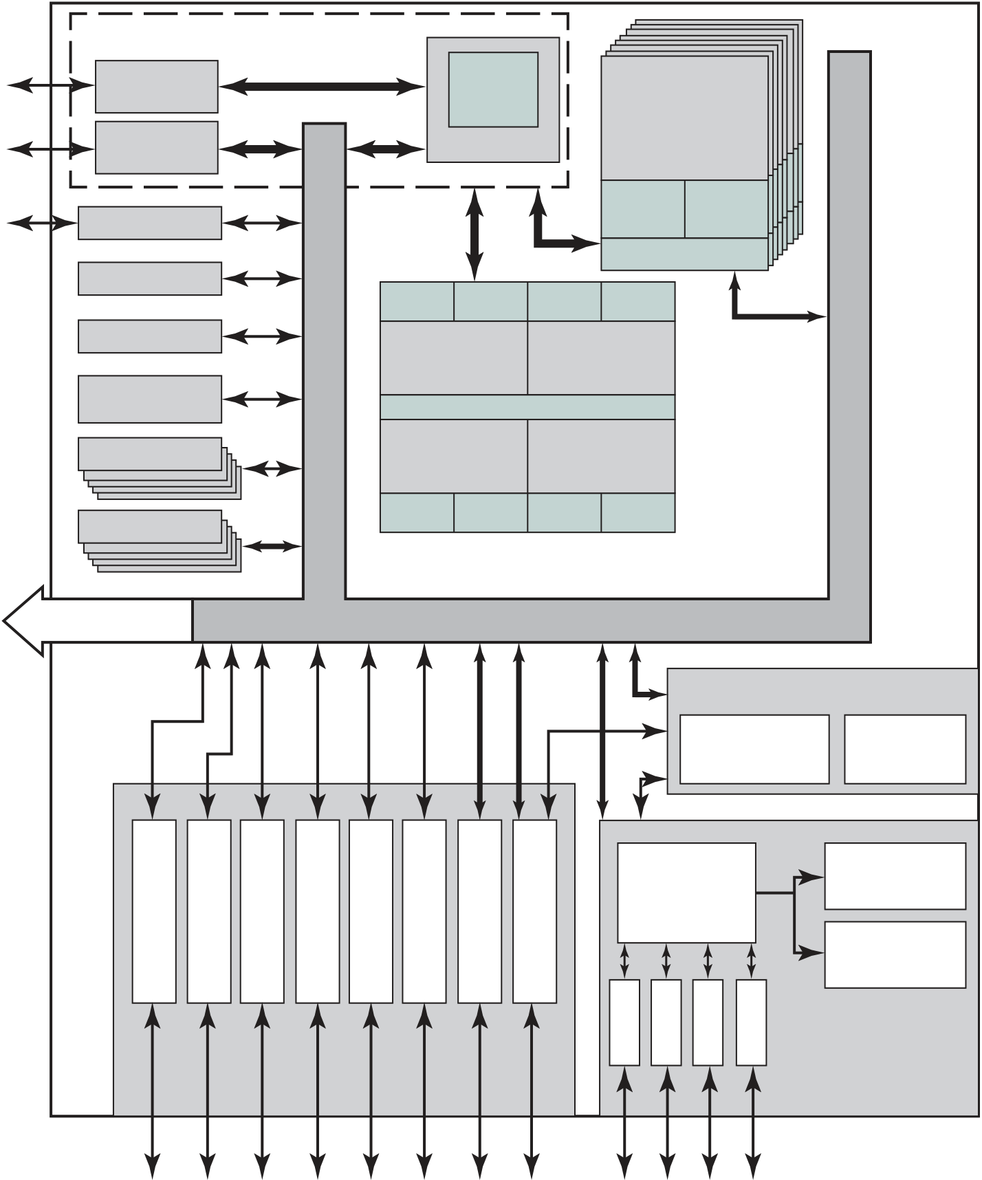
670 cHaPTer 18 / mulTIcore comPuTers
| EMIF16 | GPIO x32 | 3xI2C | USB 3.0 | 2x UART | 3x SPI | PCIe x2 | SRIO x4 |
|
Queue | Packet | ||
|---|---|---|---|---|---|---|---|---|---|---|---|---|
| manager | DMA | |||||||||||
| 5-port Ethernet switch |
|
|||||||||||
|
||||||||||||
|
||||||||||||
18.4 / HeTerogeneous mulTIcore organIzaTIon 671
Another recent approach to heterogeneous multicore organization is the use of multiple cores that have equivalent ISAs but vary in performance or power effi-ciency. The leading example of this is ARM’s big.Little architecture, which we exam-ine in this section.
Figure 18.9 illustrates this architecture. The figure shows a multicore pro-cessor chip containing two high- performance Cortex- A15 cores and two lower- performance, lower- power- consuming Cortex- A7 cores. The A7 cores handle less computation- intense tasks, such as background processing, playing music, sending texts, and making phone calls. The A15 cores are invoked for high intensity tasks, such as for video, gaming, and navigation.
CCI-400 (cache coherent interconnect)
with typically longer periods of low processing- intensity tasks, such as texting, e- mail, and audio. The big.Little architecture takes advantage of this variation in required performance. The A15 is designed for maximum performance within the mobile power budget. The A7 processor is designed for maximum efficiency and high enough performance to address all but the most intense periods of work.
a7 anda15 characteristics The A7 is far simpler and less powerful than the A15. But its simplicity requires far fewer transistors than does the A15’s complexity— and fewer transistors require less energy to operate. The differences between the A7 and A15 cores are seen most clearly by examining their instruction pipelines, as shown in Figure 18.10.
| Fetch | Decode |
|---|
Dual issue
Load/Store
Integer
Store
(b) Cortex A-15 Pipeline
The energy consumed by the execution of an instruction is partially related to the number of pipeline stages it must traverse. Therefore, a significant difference in energy consumption between Cortex- A15 and Cortex- A7 comes from the different pipeline complexity. Across a range of benchmarks, the Cortex- A15 delivers roughly twice the performance of the Cortex- A7 per unit MHz, and the Cortex- A7 is roughly three times as energy efficient as the Cortex- A15 in completing the same workloads [JEFF12]. The performance tradeoff is illustrated in Figure 18.11 [STEV13].
softwareprocessingmodels The big.Little architecture can be configured to use one of two software processing models: migration and multiprocessing (MP). The software models differ mainly in the way they allocate work to big or Little cores during runtime execution of a workload.
Highest Cortex-A7 operating point
Lowest Cortex-A7 operating point
These operating points affect the voltage and frequency of a single CPU clus-ter; however, in a big.Little system there are two CPU clusters with independent voltage and frequency domains. This allows the big cluster to act as a logical exten-sion of the DVFS operating points provided by the Little processor cluster. In a big.Little system under a migration mode of control, when Cortex- A7 is executing, the DVFS driver can tune the performance of the CPU cluster to higher levels. Once Cortex- A7 is at its highest operating point, if more performance is required, a task migration can be invoked that picks up the OS and applications and moves them to the Cortex- A15. In today’s smartphone SoCs, DVFS drivers like cpu_freq sample the OS performance at regular and frequent intervals, and the DVFS gov-ernor decides whether to shift to a higher or lower operating point or remain at the current operating point.
The migration model is simple but requires that one of the CPUs in each pair is always idle. The MP model allows any mixture of A15 and A7 cores to be powered on and executing simultaneously. Whether a big processor needs to be powered on is determined by performance requirements of tasks currently executing. If there are demanding tasks, then a big processor can be powered on to execute them. Low demand tasks can execute on a Little processor. Finally, any processors that are not being used can be powered down. This ensures that cores, big or Little, are only active when they are needed, and that the appropriate core is used to execute any given workload.
As described in Chapter 17, there are two main approaches to hardware- implemented cache coherence: directory protocols and snoopy protocols. ARM has developed a hardware coherence capability called ACE (Advanced Extensible
|
|
|
|---|---|---|
| Modifed | ||
Figure 18.12 ARM ACE Cache Line States
676 cHaPTer 18 / mulTIcore comPuTers
| (a) MESIM | ||||
|---|---|---|---|---|
| Modified | Exclusive | Shared | Invalid | |
| Dirty | Clean | Clean | N/A | |
| Yes | Yes | No | N/A | |
| Yes | Yes | No | N/A | |
|
Yes | Yes | Yes | N/A |
|
Cannot read | |||
Intel has introduced a number of multicore products in recent years. In this section, we look at the Intel Core i7-990X.
The general structure of the Intel Core i7-990X is shown in Figure 18.13. Each core has its own dedicated L2 cache and the six cores share a 12-MB L3 cache. One mechanism Intel uses to make its caches more effective is prefetching, in which the hardware examines memory access patterns and attempts to fill the caches specula-tively with data that’s likely to be requested soon.
18.6 / arm corTex- a15 mPcore 677
| Core 0 | Core 1 | Core 2 | Core 3 | Core 4 |
|
||||||
|---|---|---|---|---|---|---|---|---|---|---|---|
| 32 kB | 32 kB | 32 kB | 32 kB | 32 kB | 32 kB |
|
|
||||
| L1-I | L1-D | L1-I | L1-D | L1-I | L1-D | L1-I | L1-D | L1-I | L1-D | L1-I | |
| 256 kB | 256 kB | 256 kB | 256 kB | 256 kB | |||||||
| L2 Cache | L2 Cache | L2 Cache | L2 Cache | L2 Cache | |||||||
DDR3 Memory QuickPath
Controllers Interconnect3 ×8B @ 1.33 GT/s 4 × 20B @ 6.4 GT/s
■ Generic interrupt controller (GIC): Handles interrupt detection and interrupt prioritization. The GIC distributes interrupts to individual cores.
■ Debug unit and interface: The debug unit enables an external debug host to: stop program execution; examine and alter process and coprocessor state; examine and alter memory and input/output peripheral state; and restart the processor.
■ L2 cache: The shared L2 memory system services L1 instruction and data cache misses from each core.
■ Snoop control unit (SCU): Responsible for maintaining L1/L2 cache coherency.
Snoop control unit (SCU)
Read/write Optional 2nd R/W
64-bit bus 64-bit bus■ Masking of interrupts
■ Prioritization of the interrupts
18.6 / arm corTex- a15 mPcore 679
The GIC is designed to satisfy two functional requirements:
■ An interrupt can be directed to a specific processor only.
■ An interrupt can be directed to a defined group of processors. The MPCore views the first processor to accept the interrupt, typically the least loaded, as being best positioned to handle the interrupt.
■ Pending: A Pending interrupt is one that has been asserted, and for which processing has not started on that CPU.
■ Active: An Active interrupt is one that has been started on that CPU, but pro-cessing is not complete. An Active interrupt can be pre- empted when a new interrupt of higher priority interrupts A15 core interrupt processing.
■ Private timer and/or watchdog interrupts: These use interrupt IDs 29 and 30.
■ Legacy FIQ line: In legacy IRQ mode, the legacy FIQ pin, on a per CPU basis, bypasses the Interrupt Distributor logic and directly drives interrupt requests into the CPU.
|
|
|---|
A15 Core 0
|
Interrupt number | |||
|---|---|---|---|---|
| A15 Core 1 | ||||
| Interrupt number | ||||
A15 Core 2
Interrupt number Priority
l1 cachecoherency The L1 cache coherency scheme is based on the MESI protocol described in Chapter 17. The SCU monitors operations with shared data to optimize MESI state migration. The SCU introduces three types of optimization: direct data intervention, duplicated tag RAMs, and migratory lines.
Direct data intervention(DDI) enables copying clean data from one CPU L1 data cache to another CPU L1 data cache without accessing external memory. This reduces read after read activity from the Level 1 cache to the Level 2 cache. Thus, a local L1 cache miss is resolved in a remote L1 cache rather than from access to the shared L2 cache.
3. The line is put in the shared state in both caches.
L2 Cache Coherency
In this section, we look at a mainframe computer organization that uses multicore processor chips. The example we use is the IBM zEnterprise EC12 mainframe com-puter [SHUM13, DOBO13], which began shipping in late 2010. Section 7.8 provides a general overview of the EC12, together with a discussion of its I/O structure.
Organization
| FBC1 | PU3 | SC1 | PU4 | SC0 | PU5 | FBC1 |
|---|---|---|---|---|---|---|
| FBC2 | FBC2 |
Figure 18.16 IBM EC12 Processor Node Structure
Cache Structure
The EC12 incorporates a four- level cache structure. We look at each level in turn (Figure 18.17).
| Core | L1 | PU0 | Core | MCM | PU5 | Core | ||||||||
|---|---|---|---|---|---|---|---|---|---|---|---|---|---|---|
| 6 cores | L1: 64-kB I-cache, 96-kB D-cache | 6 cores | ||||||||||||
| D | I |
|
I | D | I | L1 |
|
I | ||||||
| D | I | L2 | L3 | L2 | D | I | L2: 1-MB I-cache, 1-MB D-cache | D | I | L2 | L3 | L2 | D | I |
| SC0 | 48 MB | L4 | L4 | 48 MB | SC1 | |||||||||
| 192 MB | ||||||||||||||
Finally, all 6 PUs on an MCM share a 160-MB L4 cache, which is split into one 92-MB cache on each SC chip. The principal motivation for incorporating a level 4 cache is that the very high clock speed of the core processors results in a significant mismatch with main memory speed. The fourth cache layer is needed to keep the cores running efficiently. The large shared L3 and L4 caches are suited to transaction- processing workloads exhibiting a high degree of data sharing and task swapping. The L4 cache is 24-way set associative. The SC chip, which houses the L4 cache, also acts as a cross- point switch for L4- to- L4 traffic to up to three remote books2 by three bidi-rectional data buses. The L4 cache is the coherence manager, meaning that all mem-ory fetches must be in the L4 cache before that data can be used by the processor. All four caches use a line size of 256 bytes.
The EC12 is an interesting study in design trade- offs and the difficulty in exploiting the increasingly powerful processors available with current technology. The large L4 cache is intended to drive the need for access to main memory down to the bare minimum. However, the distance to the off- chip L4 cache costs a num-ber of instruction cycles. Thus, the on- chip area devoted to cache is as large as possible, even to the point of having fewer cores than possible on the chip. The L1 caches are small, to minimize distance from the core and ensure that access can occur in one cycle. Each L2 cache is dedicated to a single core, in an attempt to maximize the amount of cached data that can be accessed without resort to a shared cache. The L3 cache is shared by all four cores on a chip and is as large as possible, to minimize the need to go to the L4 cache.
18.8 KEY TERMS, REVIEW QUESTIONS, AND PROBLEMS
Key Terms
|
|
|---|
Problems
| Speedup | 1 | |
|---|---|---|
| = | f * r | |
| perf(r)+ | perf(r) * n |
are available in a document at this book’s Premium Content site ( multicore- performance.pdf). What conclusions can you draw?
c. Repeat part (b) for n = 256.
}
■ |
|
|---|
ing the entire loop.
c. Could we reach peak performance running this program using fewer threads by rearranging the instructions? Explain briefly.
d. What will be the peak performance in flops/cycle for this program?
| M | O | E | S | I | |
|---|---|---|---|---|---|
|
|||||
|
|||||


19.2 GPU versus CPU
Basic Differences between CPU and GPU Architectures Performance and Performance per Watt Comparison19.3 GPU Architecture Overview
Baseline GPU Architecture
Full Chip Layout
Streaming Multiprocessor Architecture Details
Importance of Knowing and Programming to Your Memory Types
19.1 / CUDA BAsiCs 689
|
|---|
Over the past several years, the GPU has found its way into massively parallel programming environments for a wide range of applications, such as bioinformat-ics, molecular dynamics, oil and gas exploration, computational finance, signal and audio processing, statistical modeling, computer vision, and medical imaging. This is where the term general- purpose computing using a GPU (GPGPU) is derived from. The main reasons for the migration of highly parallelizable applications to the GPU are due to the advent of programmer friendly GPGPU languages, such as NVIDIA’s CUDA and the Khronos Group’s OpenCL, some slight modifications to the GPU architecture to facilitate general- purpose computing [SAND10] (from here on known as GPGPU architecture), along with the low cost and high perform-ance of GPUs. For example, for about $200, one can purchase a GPU with 960 parallel processor cores for your workstation (e.g., NVIDIA’s GeForce GTX 660).
We begin this chapter with an overview of the CUDA model, which is essen-tial for understanding the design and use of GPUs. Next, the chapter contrasts GPUs and CPUs. This is followed by a detailed look at GPU architecture. Then, Intel’s GPU is examined. Finally, the chapter discusses when to use a GPU as a coprocessor.
is difficult to describe the hardware portion of the GPGPU system without first laying the foundation with CUDA software terminology and its programming framework. These concepts will carry over into the GPU/GPGPU architecture domain.
CUDA C is a C/C++ based language. A CUDA program can be divided into three general sections: (1) code to be run on the host (CPU); (2) code to be run on the device (GPU); and (3) the code related to the transfer of data between the host and the device. The code to be run on the host is of course serial code that can’t, or isn’t worth, parallelizing. The data- parallel code to be run on the GPU is called a kernel, while a thread is a single instance of this kernel function. The kernel typi-cally will have few to no branching statements. Branching statements in the kernel result in serial execution of the threads in the GPU hardware. More about this will be covered in Section 19.3.
Block (1,1)
| Thread (0, 0) | Thread (1, 0) | Thread (2, 0) |
|
|---|---|---|---|
| Thread (0, 1) | Thread (1, 1) | Thread (2, 1) | |
| Thread (0, 2) | Thread (1, 2) | Thread (2, 2) |
Table 19.1 CUDA Terms to GPU’s Hardware Components Equivalence Mapping
Because the GPU and the CPU are designed and optimized for two significantly dif-ferent types of applications, their architectures differ significantly. This can be seen by comparing the relative amount of die area (transistor count) that is dedicated to cache, control logic, and processing logic for the two types of processor technologies (see Figure 19.2). In the CPU, as discussed in Chapter 18, the control logic and cache memory make up the majority of the CPU’s real estate. This is as expected for an architecture which is tuned to process sequential code as quickly as possible. On the other hand, a GPU uses a massively parallel SIMD (single instruction multiple data) architecture to perform mainly mathematical operations. As such, a GPU doesn’t require the same complex capabilities of the CPU’s control logic (i.e., out of order execution, branch prediction, data hazards, etc.). Nor does it require large amounts of cache memory. GPUs simply run the same thread of code on large amounts of data
692 CHAPTER 19 / EeERAal-PURPpsE RAPHiC PRpCEssie UeiTs
| DRAM |
|---|
The video game market has driven the need for ever- increasing real- time graph-ics realism. This translates into more parallel GPU processor cores with greater floating- point capabilities. As a result, the GPU is designed to maximize the num-ber of floating- point operations per second (FLOPs) it can perform. Additionally, newer NVIDIA architectures, such as the Kepler and Maxwell architectures, have focused on increasing the performance per watt ratio (FLOPs/watt) over previous GPU architectures by decreasing the power required by each GPU processor core. This was accomplished with Kepler by decreasing its processor cores’ clock, while increasing the number of on- chip transistors (following Moore’s Law) allowing for a positive net gain of 3x the performance per watt over the Fermi architecture. Addi-tionally, the Maxwell architecture has improved execution efficiency. This trend of increasing FLOPs that a GPU can perform versus a multicore CPU has diverged at an exponential rate (see Figure 19.3 [NVID14]), thus creating a large performance gap. Similar can be said about the performance per watt gap between these two dif-ferent processing technologies.
19.3 GPU ARCHITECTURE OVERVIEW
5500
5000
3000
2500
Figure 19.3 Floating- Point Operations per Second for CPU and GPU
694 CHAPTER 19 / EeERAal-PURPpsE RAPHiC PRpCEssie UeiTs
of GPU technologies, such as SMX for Kepler and SMM for Maxwell. This helps signify a relatively significant change to the SM architecture from its predecessor (it also helps with the new product’s promotional marketing!). With that being said, from a CUDA programming perspective, all of these processing technologies still have identical top- level architectures.
| Host interface | |||||||||||||||||||||||||||||||||||||||||||||||||
| L2 cache | |||||||||||||||||||||||||||||||||||||||||||||||||
| GigaThread | |||||||||||||||||||||||||||||||||||||||||||||||||
| DRAM | |||||||||||||||||||||||||||||||||||||||||||||||||
Figure 19.4 NVIDIA Fermi Architecture
|
|---|
Figure 19.5 Single SM Architecture
rate, a DDR memory designed specifically for graphic processing) DRAM, allowing for support of up to a total of 6 GB of SM off- chip memory (i.e., global, constant, texture, and local). More specifics about these different memory types will be dis-cussed in the next section. Also, illustrated in Figure 19.4 is the host interface, which can be found on the left- hand side of the GPU layout diagram. The host interface allows for PCIe connectivity between the GPU and the CPU. Lastly, the GigaThread global scheduler, in orange and located next to the host interface, is responsible for the distribution of thread blocks to all of the SM’s warp schedulers (see Figure 19.5).
696 CHAPTER 19 / EeERAal-PURPpsE RAPHiC PRpCEssie UeiTs
The GPU is most efficient when it is processing as many warps as possible to keep the CUDA cores maximally utilized. As illustrated in Figure 19.6, maximum SM hardware utilization will occur when the dual warp schedulers and instruction dispatch units are able to issue two warps every two clock cycles (Fermi architec-ture). As explained next, structural hazards are the main source of an SM falling short of achieving this maximum processing rate, while off- chip memory access latency can be more easily hidden.
Each divided column of 16 CUDA cores (* 2), 16 load/store units, and 4 SFUs (see Figure 19.5) is eligible to be assigned half a warp (16 threads) to process from each of the two warp scheduler/dispatch units per clock cycle, given that the compo-nent column isn’t experiencing a structural hazard. Structural hazards are caused by limited SFUs, double- precision multiplication, and branching. However, the warp schedulers have a built- in scoreboard to track warps that are available for execu-tion, as well as structural hazards. This allows for the SM to both work around structural hazards and help hide off- chip memory access latency as optimally as possible.
Warp 2 instruction 42 Warp 3 instruction 33
Warp 14 instruction 95 Warp 15 instruction 95
19.3 / PU ARCHiTECTURE pvERviEw 697
Therefore, it is important for the programmer to set the thread block size greater than the total number of CUDA cores in an SM, but less than the maximum allowable threads per block, and to make sure the thread block size (in the x and/ or y dimensions) is a multiple of 32 (warp size) to achieve near- optimal utilization of the SMs.
registers, sharedmemory, andl1 cache As illustrated in Figure 19.5, each SM has its own ( on- chip) dedicated set of registers and shared memory/L1 cache block. Details and benefits as to these low latency, on- chip memories are described below.
698 CHAPTER 19 / EeERAal-PURPpsE RAPHiC PRpCEssie UeiTs
| Memory Type | Access Type | Scope | Data Lifetime | |
|---|---|---|---|---|
| R/W |
|
|
||
| R/W | ||||
|
|
R/W | ||
|
R/W | |||
|
R |
|
||
| R |
|
|
19.3 / PU ARCHiTECTURE pvERviEw 699
128 kB register fle
(a) SM memory architecture
| SM 0 | SM 1 | SM 15 |
|---|
768 kB L2 cache
Although the use of shared memory will give the optimum run times, in some applications the memory accesses are not known during the programming phase. This is where having more L1 cache available (maximum setting of 48 kB) will give the optimal results. Additionally, the L1 cache helps with aiding register spills,
For example, with the GPU architecture, each thread assigned to a CUDA core has its own set of registers, such that one thread cannot access another thread’s registers, whether in the same SM or not. The only way threads within a particular SM can cooperate with each other (via data sharing) is through the shared memory (see Figure 19.8). This is typically accomplished by the programmer assigning only certain threads of an SM to write to specific locations of its shared memory, thus preventing write hazards or wasted cycles (e.g., many threads reading the same data
(Device) Grid
Global
memoryHost
from global memory and writing it to the same shared memory address). Before all of the threads of a particular SM are allowed to read from the shared memory that has just been written to, synchronization of all the threads of that SM needs to take place to prevent a read- after- write (RAW) data hazard.1
19.4 INTEL’S GEN8 GPU
Figure 19.9 Intel Gen8 Execution Unit
1See Chapter 16 for a discussion of RAW hazards.
| Instruction | Local thread | EU |
|---|---|---|
| cache | dispatcher | |
| EU | ||
| EU |
|
EU |
| EU | EU | |
| EU | EU | |
| Sampler |
|
|
| L1 | ||
EUs are organized into a subslice (Figure 19.10), which may contain up to eight EUs. Each subslice contains its own local thread dispatcher unit and its own supporting instruction caches. Thus, a single subslice has dedicated hardware resources and register files for a total of 56 simultaneous threads.
A subslice also includes a unit called the sampler, with its own local L1 and L2 cache. The sampler is used for sampling texture and image surfaces. The sam-pler includes logic to support dynamic decompression of block compression texture formats. The sampler also includes fixed- function logic that enables address conver-sion of image (u,v) coordinates and address clamping modes such as mirror, wrap, border, and clamp. The sampler supports a variety of sampling filtering modes such as point, bilinear, trilinear, and anisotropic. The data port provides efficient read/ write operations that attempt to take advantage of cache line size to consolidate read operations from different threads.
Fixed-function units
Figure 19.11 Intel Gen8 Slice
submission, as well as fixed- function logic to support 3D rendering and media pipe-lines. Additionally, the entire Gen8 compute architecture interfaces to the rest of the SoC components via a dedicated unit called the graphics technology interface (GTI).
An example of such an SoC is the Intel Core M Processor with Intel HD Graphics 5300 Gen8 (Figure 19.12). In addition to the GPU portion, the chip con-tains multiple CPU cores, an LLC cache and a system agent. The system agent includes controllers for DRAM memory, display, and PCIe devices. The Processor Graphics Gen8, CPUs, LLC cache, and system agent are interconnected with a ring structure, such as we saw for the Xeon processor (Figure 7.16).
Intel Core M Processor
Figure 19.12 Intel Core M Processor SoC
19.6 KEY TERMS AND REVIEW QUESTIONS
Key Terms
19.1 Define CUDA.
19.2 List the basic differences between CPU and GPU architectures.
Part SixThe ConTrol
UniT
CHAPTER
20.4 Key Terms, Review Questions, and Problems
707
In Chapter 12, we pointed out that a machine instruction set goes a long way toward defining the processor. If we know the machine instruction set, including an under-standing of the effect of each opcode and an understanding of the addressing modes, and if we know the set of user- visible registers, then we know the functions that the processor must perform. This is not the complete picture. We must know the exter-nal interfaces, usually through a bus, and how interrupts are handled. With this line of reasoning, the following list of those things needed to specify the function of a processor emerges:
5. Memory module interface
6. Interrupts
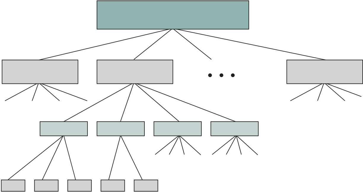
20.1 / iCRoo-oPERATionn 709
We begin by looking at the fetch cycle, which occurs at the beginning of each instruc-tion cycle and causes an instruction to be fetched from memory. For purposes of discussion, we assume the organization depicted in Figure 14.6 (Data Flow, Fetch Cycle). Four registers are involved:
■ Memory address register (MAR): Is connected to the address lines of the sys- tem bus. It specifies the address in memory for a read or write operation.
| Instruction cycle | Instruction cycle | ||||||
|---|---|---|---|---|---|---|---|
| Fetch | Indirect | Execute | |||||
| μOP | μOP | μOP |
|
|
|||
Let us look at the sequence of events for the fetch cycle from the point of view of its effect on the processor registers. An example appears in Figure 20.2. At the beginning of the fetch cycle, the address of the next instruction to be executed is in the program counter (PC); in this case, the address is 1100100. The first step is to move that address to the memory address register (MAR) because this is the only register connected to the address lines of the system bus. The second step is to bring in the instruction. The desired address (in the MAR) is placed on the address bus, the control unit issues a READ command on the control bus, and the result appears on the data bus and is copied into the memory buffer register (MBR). We also need to increment the PC by the instruction length to get ready for the next instruction. Because these two actions (read word from memory, increment PC) do not inter-fere with each other, we can do them simultaneously to save time. The third step is to move the contents of the MBR to the instruction register (IR). This frees up the MBR for use during a possible indirect cycle.
Thus, the simple fetch cycle actually consists of three steps and four micro- operations. Each micro- operation involves the movement of data into or out of a register. So long as these movements do not interfere with one another, several of them can take place during one step, saving time. Symbolically, we can write this sequence of events as follows:
■ Second time unit: Move contents of memory location specified by MAR to MBR. Increment by I the contents of the PC.
■ Third time unit: Move contents of MBR to IR.
2. Conflicts must be avoided. One should not attempt to read to and write from the same register in one time unit, because the results would be unpredictable. For example, the micro- operations (MBR d Memory) and (IR d MBR) should not occur during the same time unit.
A final point worth noting is that one of the micro- operations involves an addition. To avoid duplication of circuitry, this addition could be performed by the ALU. The use of the ALU may involve additional micro- operations, depending on the functionality of the ALU and the organization of the processor. We defer a discussion of this point until later in this chapter.
The address field of the instruction is transferred to the MAR. This is then used to fetch the address of the operand. Finally, the address field of the IR is updated from the MBR, so that it now contains a direct rather than an indirect address.
712 CHAPTER 20 / ConTRol UniT oPERATion
In the first step, the contents of the PC are transferred to the MBR, so that they can be saved for return from the interrupt. Then the MAR is loaded with the address at which the contents of the PC are to be saved, and the PC is loaded with the address of the start of the interrupt- processing routine. These two actions may each be a single micro- operation. However, because most processors provide multiple types and/or levels of interrupts, it may take one or more additional micro- operations to obtain the Save_Address and the Routine_Address before they can be transferred to the MAR and PC, respectively. In any case, once this is done, the final step is to store the MBR, which contains the old value of the PC, into memory. The processor is now ready to begin the next instruction cycle.
The Execute Cycle
ADD R1, X
which adds the contents of the location X to register R1. The following sequence of micro- operations might occur:
Let us look at two more complex examples. A common instruction is incre-ment and skip if zero:
ISZ X
BSA X
The address of the instruction that follows the BSA instruction is saved in location X, and execution continues at location X + I. The saved address will later be used for return. This is a straightforward technique for supporting subroutine calls. The following micro- operations suffice:
To complete the picture, we need to tie sequences of micro- operations together, and this is done in Figure 20.3. We assume a new 2-bit register called the instruction cycle code (ICC). The ICC designates the state of the processor in terms of which portion of the cycle it is in:
00: Fetch
01: Indirect
| Setup | ICC? | 00 (fetch) | No | Fetch | ||
|---|---|---|---|---|---|---|
| 10 (execute) |
|
|||||
| Opcode | Read | |||||
| interrupt | address | instruction | ||||
| ICC = 00 | Execute | ICC = 10 | Indirect | |||
| instruction |
addressing?
At the end of each of the four cycles, the ICC is set appropriately. The indirect cycle is always followed by the execute cycle. The interrupt cycle is always followed by the fetch cycle (see Figure 14.4, The Instruction Cycle). For both the fetch and execute cycles, the next cycle depends on the state of the system.
Thus, the flowchart of Figure 20.3 defines the complete sequence of micro- operations, depending only on the instruction sequence and the interrupt pattern. Of course, this is a simplified example. The flowchart for an actual processor would be more complex. In any case, we have reached the point in our discussion in which the operation of the processor is defined as the performance of a sequence of micro- operations. We can now consider how the control unit causes this sequence to occur.
With the information at hand, the following three- step process leads to a char-acterization of the control unit:
1. Define the basic elements of the processor.
■ Registers
■ Internal data paths
■ Transfer data from one register to another.
■ Transfer data from a register to an external interface (e.g., system bus).
■ Sequencing: The control unit causes the processor to step through a series of micro- operations in the proper sequence, based on the program being executed.
■ Execution: The control unit causes each micro- operation to be performed.
We have defined the elements that make up the processor (ALU, registers, data paths) and the micro- operations that are performed. For the control unit to perform its function, it must have inputs that allow it to determine the state of the system and outputs that allow it to control the behavior of the system. These are the external specifications of the control unit. Internally, the control unit must have the logic required to perform its sequencing and execution functions. We defer a discussion of the internal operation of the control unit to Section 20.3 and Chapter 21. The remainder of this section is concerned with the interaction between the control unit and the other elements of the processor.
Figure 20.4 is a general model of the control unit, showing all of its inputs and outputs. The inputs are:
Instruction register
Control signals
within CPU
| Flags | Control | Control signals | |
|---|---|---|---|
| from control bus | |||
| unit |
The outputs are as follows:
■ Control signals within the processor: These are two types: those that cause data to be moved from one register to another, and those that activate specific ALU functions.
■ A memory read control signal on the control bus;
■ A control signal that opens the gates, allowing the contents of the data bus to be stored in the MBR;
A Control Signals Example
To illustrate the functioning of the control unit, let us examine a simple example. Figure 20.5 illustrates the example. This is a simple processor with a single accu-mulator (AC). The data paths between elements are indicated. The control paths for signals emanating from the control unit are not shown, but the terminations of control signals are labeled Ci and indicated by a circle. The control unit receives inputs from the clock, the IR, and flags. With each clock cycle, the control unit
| C0 | C2 | C13 | ALU | Control | |
|---|---|---|---|---|---|
| signals |
A
■ ALU: The control unit controls the operation of the ALU by a set of control signals. These signals activate various logic circuits and gates within the ALU.
■ System bus: The control unit sends control signals out onto the control lines of the system bus (e.g., memory READ).
| Micro- operations | Active Control Signals | |
|---|---|---|
|
|
|
|
||
|
||
|
|
|
|
|
Two new registers, labeled Y and Z, have been added to the organization. These are needed for the proper operation of the ALU. When an operation involv-ing two operands is performed, one can be obtained from the internal bus, but the other must be obtained from another source. The AC could be used for this pur-pose, but this limits the flexibility of the system and would not work with a proces-sor with multiple general- purpose registers. Register Y provides temporary storage for the other input. The ALU is a combinatorial circuit (see Chapter 11) with no internal storage. Thus, when control signals activate an ALU function, the input to the ALU is transformed to the output. Therefore, the output of the ALU cannot be directly connected to the bus, because this output would feed back to the input. Register Z provides temporary output storage. With this arrangement, an operation to add a value from memory to the AC would have the following steps:
t1: MAR d (IR(address))
t2: MBR d Memory
t3: Y d (MBR)
t4: Z d (AC) + (Y)
t5: AC d (Z)
IR
PC
Figure 20.6 CPU with Internal Bus
interconnection layout and the control of the processor. Another practical reason for the use of an internal bus is to save space.
■ Serial I/O control: This module interfaces to devices that communicate 1 bit at a time.
Table 20.2 describes the external signals into and out of the 8085. These are linked to the external system bus. These signals are the interface between the 8085 processor and the rest of the system (Figure 20.8).
| INTA | RST 6.5 | SID | ||||
|---|---|---|---|---|---|---|
| INTR | RST 5.5 |
|
||||
| Interrupt control |
|
|||||
| Power | Clk |
|
(8) | (8) | |||||||||
|---|---|---|---|---|---|---|---|---|---|---|---|---|---|
| supply | |||||||||||||
| X1 | |||||||||||||
| X2 | |||||||||||||
| Gen | Control | Status | DMA | Reset |
|
address buffer | |||||||
| RD WR | ALE | S0 S1 |
|
Reset out | |||||||||
| Ready | |||||||||||||
| Hold |
|
||||||||||||
722 CHAPTER 20 / ConTRol UniT oPERATion Table 20.2 Intel 8085 External Signals
|
|---|
Figure 20.8 Intel 8085 Pin Configuration
| 3-MHz | T1 | T2 | M1 | T4 | T1 | M2 | T3 | T1 | M3 | T3 | |
|---|---|---|---|---|---|---|---|---|---|---|---|
| T2 | T2 |
ALE
RD
Figure 20.9 Timing Diagram for Intel 8085 OUT Instruction
to be placed on the address bus (A15 through A8) and the address/data bus (AD7 through AD0). With the falling edge of the ALE pulse, the other modules on the bus store the address.
■ Microprogrammed implementation
In a hardwired implementation, the control unit is essentially a state machine circuit. Its input logic signals are transformed into a set of output logic signals, which
First consider the IR. The control unit makes use of the opcode and will per-form different actions (issue a different combination of control signals) for different instructions. To simplify the control unit logic, there should be a unique logic input for each opcode. This function can be performed by a decoder, which takes an encoded input and produces a single output. In general, a decoder will have n binary inputs and 2n binary outputs. Each of the 2n different input patterns will activate a single unique output. Table 20.3 is an example for n= 4. The decoder for a control unit will typi-cally have to be more complex than that, to account for variable- length opcodes. An example of the digital logic used to implement a decoder is presented in Chapter 11.
The clock portion of the control unit issues a repetitive sequence of pulses. This is useful for measuring the duration of micro- operations. Essentially, the period of the clock pulses must be long enough to allow the propagation of signals along
| I1 | 0 | 0 | 0 | 0 | 0 | 0 | 0 | 0 | 1 | 1 | 1 | 1 | 1 | 1 | 1 | 1 |
|---|---|---|---|---|---|---|---|---|---|---|---|---|---|---|---|---|
| I2 | 0 | 0 | 0 | 0 | 1 | 1 | 1 | 1 | 0 | 0 | 0 | 0 | 1 | 1 | 1 | 1 |
| I3 | 0 | 0 | 1 | 1 | 0 | 0 | 1 | 1 | 0 | 0 | 1 | 1 | 0 | 0 | 1 | 1 |
| I4 | 0 | 1 | 0 | 1 | 0 | 1 | 0 | 1 | 0 | 1 | 0 | 1 | 0 | 1 | 0 | 1 |
| O1 | 0 | 0 | 0 | 0 | 0 | 0 | 0 | 0 | 0 | 0 | 0 | 0 | 0 | 0 | 0 | 1 |
| O2 | 0 | 0 | 0 | 0 | 0 | 0 | 0 | 0 | 0 | 0 | 0 | 0 | 0 | 0 | 1 | 0 |
| O3 | 0 | 0 | 0 | 0 | 0 | 0 | 0 | 0 | 0 | 0 | 0 | 0 | 0 | 1 | 0 | 0 |
| O4 | 0 | 0 | 0 | 0 | 0 | 0 | 0 | 0 | 0 | 0 | 0 | 0 | 1 | 0 | 0 | 0 |
| O5 | 0 | 0 | 0 | 0 | 0 | 0 | 0 | 0 | 0 | 0 | 0 | 1 | 0 | 0 | 0 | 0 |
| O6 | 0 | 0 | 0 | 0 | 0 | 0 | 0 | 0 | 0 | 0 | 1 | 0 | 0 | 0 | 0 | 0 |
| O7 | 0 | 0 | 0 | 0 | 0 | 0 | 0 | 0 | 0 | 1 | 0 | 0 | 0 | 0 | 0 | 0 |
| O8 | 0 | 0 | 0 | 0 | 0 | 0 | 0 | 0 | 1 | 0 | 0 | 0 | 0 | 0 | 0 | 0 |
| O9 | 0 | 0 | 0 | 0 | 0 | 0 | 0 | 1 | 0 | 0 | 0 | 0 | 0 | 0 | 0 | 0 |
| O10 | 0 | 0 | 0 | 0 | 0 | 0 | 1 | 0 | 0 | 0 | 0 | 0 | 0 | 0 | 0 | 0 |
| O11 | 0 | 0 | 0 | 0 | 0 | 1 | 0 | 0 | 0 | 0 | 0 | 0 | 0 | 0 | 0 | 0 |
| O12 | 0 | 0 | 0 | 0 | 1 | 0 | 0 | 0 | 0 | 0 | 0 | 0 | 0 | 0 | 0 | 0 |
| O13 | 0 | 0 | 0 | 1 | 0 | 0 | 0 | 0 | 0 | 0 | 0 | 0 | 0 | 0 | 0 | 0 |
| O14 | 0 | 0 | 1 | 0 | 0 | 0 | 0 | 0 | 0 | 0 | 0 | 0 | 0 | 0 | 0 | 0 |
| O15 | 0 | 1 | 0 | 0 | 0 | 0 | 0 | 0 | 0 | 0 | 0 | 0 | 0 | 0 | 0 | 0 |
| O16 | 1 | 0 | 0 | 0 | 0 | 0 | 0 | 0 | 0 | 0 | 0 | 0 | 0 | 0 | 0 | 0 |
With these two refinements, the control unit can be depicted as in Figure 20.10.
Control Unit Logic
PQ = 01 Indirect Cycle
PQ = 10 Execute Cycle
Decoder
| Clock | Timing | Control | Flags | |
|---|---|---|---|---|
| generator | unit |
That is, the control signal C5 will be asserted during the second time unit of both the fetch and indirect cycles.
This expression is not complete. C5 is also needed during the execute cycle. For our simple example, let us assume that there are only three instructions that read from memory: LDA, ADD, and AND. Now we can define C5 as
20.4 KEY TERMS, REVIEW QUESTIONS, AND PROBLEMS
Key Terms
| control bus control path |
|---|
| 20.1 |
|---|
Stack
pointer
| Stack | Free | Block | Descending addresses | |
|---|---|---|---|---|
| base | In use | |||
| reserved | ||||
| for stack |
Figure 20.11 Typical Stack Organization (full/descending)
21.2 Microinstruction Sequencing
Design Considerations
Sequencing Techniques
Address Generation
LSI-11 Microinstruction Sequencing21.3 Microinstruction Execution
A Taxonomy of Microinstructions Microinstruction Encoding
LSI-11 Microinstruction Execution IBM 3033 Microinstruction Execution
The state of the microprogramming art was reviewed by Datamation in its February 1964 issue. No microprogrammed system was in wide use at that time, and one of the papers [HILL64] summarized the then-popular view that the future of microprogramming “is somewhat cloudy. None of the major manufacturers has evidenced interest in the technique, although presumably all have examined it.” This situation changed dramatically within a very few months. IBM’s Sys-tem/360 was announced in April, and all but the largest models were micropro-grammed. Although the 360 series predated the availability of semiconductor ROM, the advantages of microprogramming were compelling enough for IBM to make this move. Microprogramming became a popular technique for imple-menting the control unit of CISC processors. In recent years, microprogram-ming has become less used but remains a tool available to computer designers. For example, as we have seen on the Pentium 4, machine instructions are con-verted into a RISC-like format, most of which are executed without the use of microprogramming. However, some of the instructions are executed using microprogramming.
21.1 BASIC CONCEPTS
Consider Table 21.1. In addition to the use of control signals, each micro- operation is described in symbolic notation. This notation looks suspiciously like a programming language. In fact it is a language, known as a microprogramming language. Each line describes a set of micro-operations occurring at one time and is known as a microinstruction. A sequence of instructions is known as a micropro-gram, or firmware. This latter term reflects the fact that a microprogram is midway between hardware and software. It is easier to design in firmware than hardware, but it is more difficult to write a firmware program than a software program.
How can we use the concept of microprogramming to implement a control unit? Consider that for each micro-operation, all that the control unit is allowed to do is generate a set of control signals. Thus, for any micro-operation, each con-trol line emanating from the control unit is either on or off. This condition can, of course, be represented by a binary digit for each control line. So we could construct a control word in which each bit represents one control line. Then each micro-oper-ation would be represented by a different pattern of 1s and 0s in the control word.
732 CHAPTER 21 / MiCRoPRogRAMMEd ConTRol
The result is known as a horizontal microinstruction, an example of which is shown in Figure 21.1a. The format of the microinstruction or control word is as follows. There is one bit for each internal processor control line and one bit for each system bus control line. There is a condition field indicating the condition under which there should be a branch, and there is a field with the address of the micro-instruction to be executed next when a branch is taken. Such a microinstruction is interpreted as follows:
The control memory of Figure 21.2 is a concise description of the complete operation of the control unit. It defines the sequence of micro-operations to be
Microinstruction address
Jump condition
—Unconditional
—Zero
—Overfow
—Indirect bit
System bus control signals
Internal CPU control signals
Figure 21.1 Typical Microinstruction Formats
Indirect
cycle
Interrupt
cycle
| Jump to fetch | routine |
|---|
ADD routine
Jump to fetch or interrupt
Microprogrammed Control Unit
The control memory of Figure 21.2 contains a program that describes the behavior of the control unit. It follows that we could implement the control unit by simply executing that program.
logic
Read
1. To execute an instruction, the sequencing logic unit issues a READ command to the control memory.
2. The word whose address is specified in the control address register is read into the control buffer register.
■ Get the next instruction: Add 1 to the control address register.
■ Jump to a new routine based on a jump microinstruction: Load the address field of the control buffer register into the control address register.
Instruction register
Control
| ALU | Decoder | |
|---|---|---|
| Sequencing | ||
| Flags | ||
| Clock | logic |
Control buffer register
Next address control
DecoderAs was mentioned, Wilkes first proposed the use of a microprogrammed control unit in 1951 [WILK51]. This proposal was subsequently elaborated into a more detailed design [WILK53]. It is instructive to examine this seminal proposal.
The configuration proposed by Wilkes is depicted in Figure 21.5. The heart of the system is a matrix partially filled with diodes. During a machine cycle, one row of the matrix is activated with a pulse. This generates signals at those points where a diode is present (indicated by a dot in the diagram). The first part of the row generates the con-trol signals that control the operation of the processor. The second part generates the
Clock
Register I
| Control signals |
|---|
Figure 21.5 Wilkes’s Microprogrammed Control Unit
address of the row to be pulsed in the next machine cycle. Thus, each row of the matrix is one microinstruction, and the layout of the matrix is the control memory.
21.1 / BAsiC ConCEPTs 737
|
|
Instructions 0 through 4 constitute the fetch cycle. Microinstruction 4 presents the opcode to a decoder, which generates the address of a microinstruction corre-sponding to the machine instruction to be fetched. The reader should be able to deduce the complete functioning of the control unit from a careful study of Table 21.2.
Advantages and Disadvantages
Notations: A, B, C, . . . stand for the various registers in the arithmetical and control register units. C to D indicates
that the switching circuits connect the output of register C to the input register D;(D + A) to C indicates that the output register of A is connected to the one input of the adding unit (the output of D is permanently connected to the other input), and the output of the adder to register C. A numerical symbol n in quotes (e.g., “n”) stands for the source whose output is the number n in units of the least significant digit.
21.2 / MiCRoinsTRuCTion sEquEnCing 739
|
|||||||
|---|---|---|---|---|---|---|---|
| Set | Use | 0 | 1 | ||||
| 31 | D to C | 2 | 28 | 33 | |||
| 32 | (D + A) to C | 2 | 28 | 33 | |||
| 33 | B to D | (1)B1 | 34 | ||||
| 34 | D to B (R) | 35 | |||||
| 35 | C to D (R) | 1 | 36 | 37 | |||
| 36 | D to C | 0 | |||||
| 37 | (D - A) to C | 0 | |||||
† Left shift. The switching circuits are similarly arranged to pass the most significant digit of register B to the least significant place of register C during left shift micro-operations.
21.2 MICROINSTRUCTION SEQUENCING
Design Considerations
Two concerns are involved in the design of a microinstruction sequencing technique: the size of the microinstruction and the address-generation time. The first concern is obvious; minimizing the size of the control memory reduces the cost of that com-ponent. The second concern is simply a desire to execute microinstructions as fast as possible.
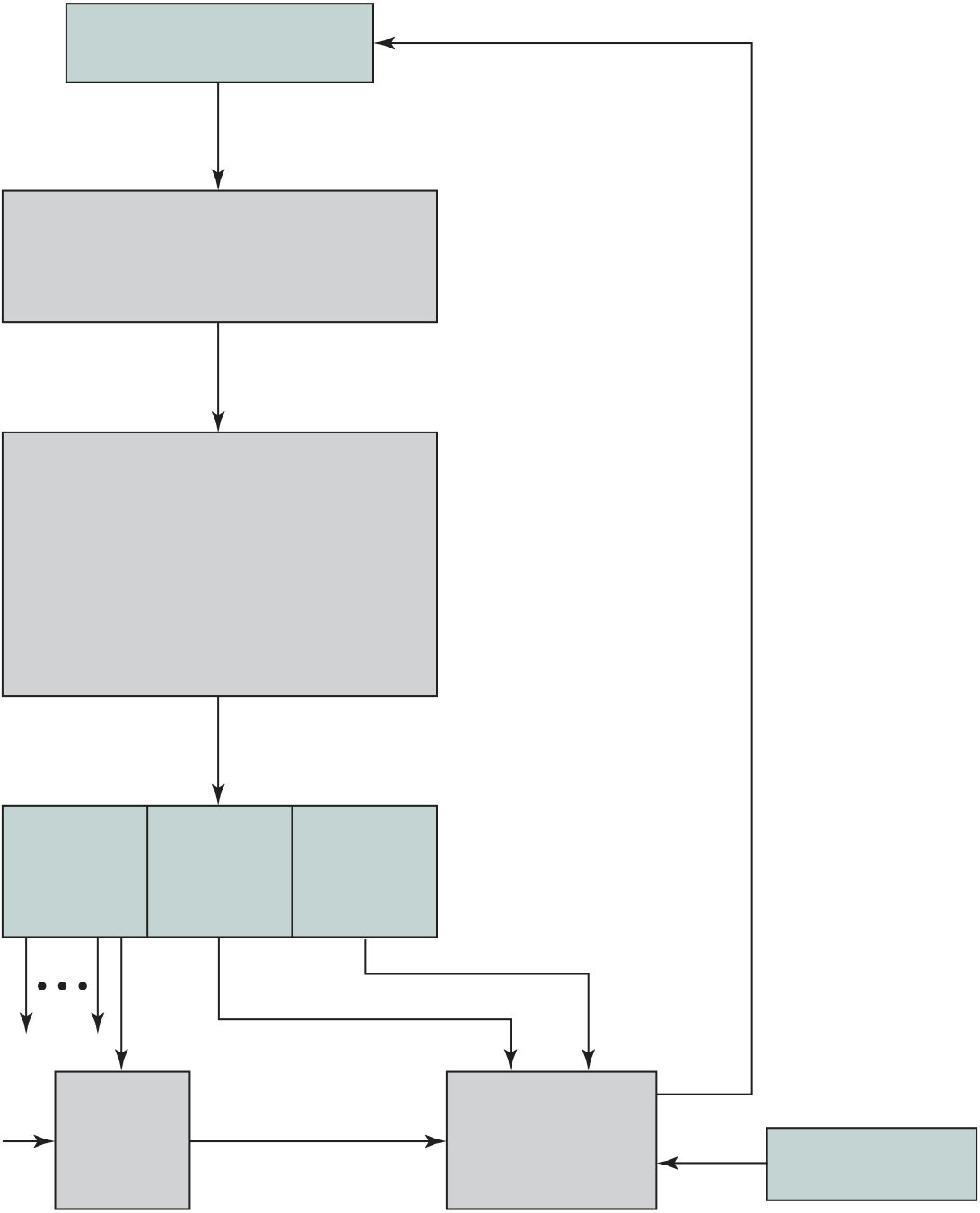
740 CHAPTER 21 / MiCRoPRogRAMMEd ConTRol
Address
decoderControl
memory
| Flags | Branch | selection |
|
Instruction |
|---|---|---|---|---|
| logic | ||||
| register |
Figure 21.6 Branch Control Logic: Two Address Fields
| Flags | Branch | Instruction | ||
|---|---|---|---|---|
| logic | ||||
| register |
■ Two address fields
■ Single address field
■ Instruction register code
■ Next sequential address
Control
buffer
| Flags | Branch | Instruction | ||
|---|---|---|---|---|
| logic | register | |||
|
Figure 21.8 Branch Control Logic: Variable Format
Address Generation
We have looked at the sequencing problem from the point of view of format con-siderations and general logic requirements. Another viewpoint is to consider the various ways in which the next address can be derived or computed.
■ Parts of a selected register, such as the sign bit
■ Status bits within the control unit
00 07 08 09 10 11 12
Figure 21.9 IBM 3033 Control Address Register
The final approach listed in Table 21.3 is termed residual control. This approach involves the use of a microinstruction address that has previously been saved in temporary storage within the control unit. For example, some microin-struction sets come equipped with a subroutine facility. An internal register or stack of registers is used to hold return addresses. An example of this approach is taken on the LSI-11, which we now examine.
■ Opcode mapping: At the beginning of each instruction cycle, the next microin- struction address is determined by the opcode.
■ Subroutine facility: Explained presently.
21.3 / MiCRoinsTRuCTion ExECuTion 745
As can be seen, the LSI-11 includes a powerful address sequencing facility within the control unit. This allows the microprogrammer considerable flexibility and can ease the microprogramming task. On the other hand, this approach requires more control unit logic than do simpler capabilities.
The control logic module generates control signals as a function of some of the bits in the microinstruction. It should be clear that the format and content of the microinstruction determines the complexity of the control logic module.
A Taxonomy of Microinstructions
■ Direct/indirect encoding
All of these bear on the format of the microinstruction. None of these terms has been used in a consistent, precise way in the literature. However, an examination of these pairs of qualities serves to illuminate microinstruction design alterna-tives. In the following paragraphs, we first look at the key design issue underlying all of these pairs of characteristics, and then we look at the concepts suggested by each pair.
|
|
|
|---|---|---|
| Clock |
Figure 21.10 Control Unit Organization
sequencing schemes, using fewer microinstruction bits, are possible. These schemes require a more complex sequencing logic module. A similar sort of trade-off exists for the portion of the microinstruction concerned with control signals. By encoding control information, and subsequently decoding it to produce control signals, con-trol word bits can be saved.
■ Only one pattern of control signals can be presented to the external control bus at a time.
21.3 / MiCRoinsTRuCTion ExECuTion 747
■ More bits than are strictly necessary are used to encode the possible combinations.
■ Some combinations that are physically allowable are not possible to encode.
Table 21.4 The Microinstruction Spectrum
| Characteristics |
|---|
|
| Terminology |
748 CHAPTER 21 / MiCRoPRogRAMMEd ConTRol
by the microprogrammer. Encoding is done in such a way as to aggregate functions or resources, so that the microprogrammer is viewing the processor at a higher, less detailed level. Furthermore, the encoding is designed to ease the microprogram-ming burden. Again, it should be clear that the task of understanding and orches-trating the use of all the control signals is a difficult one. As was mentioned, one of the consequences of encoding, typically, is to prevent the use of certain otherwise allowable combinations.
The other pair of terms mentioned at the beginning of this subsection refers to direct versus indirect encoding, a subject to which we now turn.
Microinstruction Encoding
Let us consider the implications of this layout. When the microinstruction is executed, every field is decoded and generates control signals. Thus, with N fields, N simultaneous actions are specified. Each action results in the activation of one or more control signals. Generally, but not always, we will want to design the format so that each control signal is activated by no more than one field. Clearly, however, it must be possible for each control signal to be activated by at least one field.
Now consider the individual field. A field consisting of L bits can contain one of 2L codes, each of which can be encoded to a different control signal pattern. Because only one code can appear in a field at a time, the codes are mutually exclu-sive, and, therefore, the actions they cause are mutually exclusive.
Control signals
(a) Direct encoding
| Field | Field | Field |
|---|---|---|
Control signals
(b) Indirect encoding
■ Organize the format into independent fields. That is, each field depicts a set of actions (pattern of control signals) such that actions from different fields can occur simultaneously.
■ Define each field such that the alternative actions that can be specified by the field are mutually exclusive. That is, only one of the actions specified for a given field could occur at a time.
|
|
|
||||||||||
|
CSAR Constant (in next byte) | |||||||||||
| 0 0 0 0 1 0 | ||||||||||||
|
||||||||||||
|
|
|||||||||||
|
||||||||||||
|
||||||||||||
|
||||||||||||
| 0 |
|
|||||||||||
21.3 / MiCRoinsTRuCTion ExECuTion 751
field. For example, consider an ALU that is capable of performing eight different arithmetic operations and eight different shift operations. A 1-bit field could be used to indicate whether a shift or arithmetic operation is to be used; a 3-bit field would indicate the operation. This technique generally implies two levels of decod-ing, increasing propagation delays.
Figure 21.13 depicts, in simplified form, the organization of the LSI-11 pro-cessor. The three chips are the data, control, and control store chips. The data chip contains an 8-bit ALU, twenty-six 8-bit registers, and storage for several condition
Control
store
| 4 | 18 | 16 | ||
|---|---|---|---|---|
| bus | ||||
|
Data | With no number indicated, | ||
| chip | chip | |||
| 16 |
|
Figure 21.13 Simplified Block Diagram of the LSI-11 Processor
Figure 21.14 provides a still simplified but more detailed look at the LSI-11 control unit: the figure ignores individual chip boundaries. The address sequencing scheme described in Section 21.2 is implemented in two modules. Overall sequence control is provided by the microprogram sequence control module, which is capable
Control data register
| Instruction register | Translation | INT |
|---|---|---|
| array |
Figure 21.14 Organization of the LSI-11 Control Unit
21.3 / MiCRoinsTRuCTion ExECuTion 753
■ Interrupt conditions are periodically tested.
■ Conditional branch microinstructions are evaluated.
Load return register
Translate
(a) Format of the full LSI-11 microinstruction
| 5 | 11 | 4 | 8 | 4 |
|---|
| Opcode | Literal value | A register |
|---|
| Opcode | Test code |
|---|
Register jump microinstruction format
(b) Format of the encoded part of the LSI-11 microinstruction
are used to store 126-bit microinstructions. The format is depicted in Figure 21.16.
|
35 |
|---|
| 36 | 71 |
|---|
| 72 |
|---|
|
|
|---|---|
| 125 | |
21.4 / Ti 8800 755
Table 21.6 IBM 3033 Microinstruction Control Fields
The sequencing mechanism for the IBM 3033 was discussed in Section 21.2.
21.4 TI 8800
■ Microcode memory
■ Microsequencer
15 Next microcode address
Microcode memory
32K × 128 bits
| microinstruction | 96 |
|---|
32
|
|
|---|
The board fits into an IBM PC-compatible host computer. The host computer provides a suitable platform for microcode assembly and debug.
Microinstruction Format
■ 8818 microsequencer
■ WCS data field
■ Enabling local data memory read/write operations.
■ Determining the unit driving the system Y bus. One of the four devices attached to the bus (Figure 21.17) is selected.
The next address can be selected from one of five sources:
1. The microprogram counter (MPC) register, used for repeat (reuse same address) and continue (increment address by 1) instructions.
3. The DRA and DRB ports, which provide two additional paths from exter-nal hardware by which microprogram addresses can be generated. These two ports are connected to the most significant and least significant 16 bits of the DA bus, respectively. This allows the microsequencer to obtain the next instruction address from the WCS data field of the current microinstruction or from a result calculated by the ALU.
4. Register counters RCA and RCB, which can be used for additional address storage.
■ A 65-word by 16-bit stack, which allows microprogram subroutine calls and interrupts.
■ An interrupt return register and Y output enable for interrupt processing at the microinstruction level.
1. Clear, which sets the stack pointer to zero, emptying the stack;
2. Pop, which decrements the stack pointer;
DA31-DA16 DA15-DA00
(DRA) (DRA)
MUX
| Interrupt | Y output | |
|---|---|---|
| counter/ | return | |
| multiplexer | ||
| incrementer | register |
Next microde
addressFigure 21.18 TI 8818 Microsequencer
21.4 / Ti 8800 761
Figure 21.18). The output is selected to come from either the stack or from reg-ister RCA. DRA then serves as input to either the Y output multiplexer or to register RCA.
■ MUX2–MUX0: Output controls. These bits, together with the condition code if used, control the Y output multiplexer and therefore the next microinstruc-tion address. The multiplexer can select its output from the stack, DRA, DRB, or MPC.
These bits can be set individually by the programmer. However, this is typically not done. Rather, the programmer uses mnemonics that equate to the bit patterns that would normally be required. Table 21.8 lists the 15 mnemonics for field 28. A microcode assembler converts these into the appropriate bit patterns.
As an example, the instruction INC88181 is used to cause the next microin-struction in sequence to be selected, if the currently selected condition code is 1.
From Table 21.8, we have
■ R = 000: Retain current value of RA and RC.
■ S = 111: Retain current state of stack.
Three 6-bit address ports allow a two-operand fetch and an operand write to be performed within the register file simultaneously. An MQ shifter and MQ regis-ter can also be configured to function independently to implement double-precision 8-bit, 16-bit, and 32-bit shift operations.
Fields 17 through 26 of each microinstruction control the way in which data flows within the 8832 and between the 8832 and the external environment. The fields are as follows:
21.4 / Ti 8800 763
21. ALU Configuration Mode. The 8832 can be configured to operate as a single 32-bit ALU, two 16-bit ALUs, or four 8-bit ALUs.
26. Source Register. Address of register in register file to be used for the source operand, provided by the R multiplexer.
Finally, field 27 is an 8-bit opcode that specifies the arithmetic or logical func-tion to be performed by the ALU. Table 21.9 lists the different operations that can be performed.
■ Field [18] is changed to SELRFYMX to select the feedback from the ALU Y MUX output.
■ Field [24] is changed to designate register R3 for the destination register.
CONT11 [17],WELH,[18],SELRFYMX
can be written as
| Group 1 |
|
|
|---|---|---|
|
||
|
||
|
||
|
||
|
||
|
||
|
||
|
||
|
||
|
||
|
||
|
||
|
||
| Group 2 | ||
|
|
|
|
|
|
|
|
|
|
|
|
|
|
|
|
|
|
|
|
|
|
|
|
| Group 3 | ||
|
|
|
|
|
|
|
|
|
21.4 / Ti 8800 765
|
|
|---|
IF (AC0 = 1) THEN CAR d (C0-6) ELSE CAR d (CAR) + 1
where AC0 is the sign bit of the accumulator and C0-6 are the first seven bits of the microinstruction. Using this microinstruction, write a microprogram that implements a Branch Register Minus (BRM) machine instruction, which branches if the AC is negative. Assume that bits C1 through Cn of the microinstruction specify a parallel set of micro-operations. Express the program symbolically.
21.5 / KEy TERMs, REviEw quEsTions, And PRoBlEMs 767
21.8 |
|
|---|
Projectsfor teaching comPuter organizationand architecture
A.1 Interactive Simulations
A.2 Research Projects
A.3 Simulation Projects
SimpleScalar
SMPCache
A.4 Assembly Language Projects
A.5 Reading/Report Assignments
A.6 Writing Assignments
A.7 Test Bank
■ Interactive simulations
■ Research projects
■ Test bank
A.1 InterActIve SImulAtIonS
■ A format for the proposal
■ A format for the final report
An excellent way to obtain a grasp of the internal operation of a processor and to study and appreciate some of the design trade- offs and performance implications is by simulating key elements of the processor. Two tools that are useful for this pur-pose are SimpleScalar and SMPCache.
Compared with actual hardware implementation, simulation provides two advantages for both research and educational use:
The IRC for this book includes a concise introduction to SimpleScalar for students, with instructions on how to load and get started with SimpleScalar. The manual also includes some suggested project assignments.
772 AppendIx A / projectS for teAchIng computer orgAnIzAtIon
SMPCache is a portable software package the runs on PC systems with Win-dows. The SMPCache software can be downloaded from the SMPCache Web site. It is available at no cost for noncommercial use.
A.4 ASSembly lAnguAge ProjectS
other one is. MARS executes the programs in a simple version of time- sharing. The two programs take turns: a single instruction of the first program is executed, then a single instruction of the second, and so on. What a battle program does during the execution cycles allotted to it is entirely up to the programmer. The aim is to destroy the other program by ruining its instructions. The CodeBlue environment substi-tutes CodeBlue for Redcode and provides its own interactive execution interface.
The IRC includes the CodeBlue environment, a user’s manual for students, other supporting material, and suggested assignments.
The IRC contains a number of suggested writing assignments, organized by chapter. Instructors may ultimately find that this is the most important part of their approach to teaching the material. I would greatly appreciate any feedback on this area and any suggestions for additional writing assignments.
A.7 teSt bAnk
B.2 Assemblers
Two-Pass Assembler
One-Pass Assembler
Example: Prime Number ProgramB.3 Loading and Linking
Relocation
Loading
Linking
1. It clarifies the execution of instructions.
2. It shows how data are represented in memory.
Table B.1 defines some of the key terms used in this appendix.
B.1 AssemBly lAnguAge
1There are a number of assemblers for the x86 architecture. Our examples use NASM (Netwide Assem-bler), an open source assembler. A copy of the NASM manual is at this book’s Premium Content site.
776 Appendix B / AssemBly lAnguAge And RelAted topics
|
|---|
B.1 / AssemBly lAnguAge 777
6. System code can use intrinsic functions instead of assembly. The best modern C++ compilers have intrinsic functions for accessing system control registers and other system instructions. Assembly code is no longer needed for device drivers and other system code when intrinsic functions are available.
2. Making compilers. Understanding assembly coding techniques is necessary for making compilers, debuggers, and other development tools.
3. Embedded systems. Small embedded systems have fewer resources than PCs and mainframes. Assembly programming can be necessary for optimizing code for speed or size in small embedded systems.
8. Optimizing code for speed. Modern C++ compilers generally optimize code quite well in most cases. But there are still cases where compilers perform poorly and where dramatic increases in speed can be achieved by careful assembly programming.
9. Function libraries. The total benefit of optimizing code is higher in function libraries that are used by many programmers.
A statement in a typical assembly language has the form shown in Figure B.1. It con-sists of four elements: label, mnemonic, operand, and comment.
label If a label is present, the assembler defines the label as equivalent to the address into which the first byte of the object code generated for that instruction will be loaded. The programmer may subsequently use the label as an address or as data in another instruction’s address field. The assembler replaces the label with the assigned value when creating an object program. Labels are most frequently used in branch instructions.
;positive
The program will continue to loop back to location L2 until the result is zero or negative. Thus, when the jg instruction is executed, if the result is positive, the processor places the address equivalent to the label L2 in the program counter.
| Optional | Opcode name | Zero or more |
|---|
mnemonic The mnemonic is the name of the operation or function of the assembly language statement. As discussed subsequently, a statement can correspond to a machine instruction, an assembler directive, or a macro. In the case of a machine instruction, a mnemonic is the symbolic name associated with a particular opcode.
Table 12.8 lists the mnemonic, or instruction name, of many of the x86 instruc-tions. Appendix A of [CART06] lists the x86 instructions, together with the oper-ands for each and the effect of the instruction on the condition codes. Appendix B of the NASM manual provides a more detailed description of each x86 instruction. Both documents are available at this book’s Premium Content site.
MOV [3518H], AX
First the 16-bit register AX is initialized to 1234H. Then, in line two, the contents of AX are moved to the logical address DS:3518H. This address is formed by shifting the contents of DS left 4 bits and adding 3518H to form the 32-bit logical address 13518H.
directives Directives, also called pseudo-instructions, are assembly language statements that are not directly translated into machine language instructions. Instead, directives are instruction to the assembler to perform specified actions doing the assembly process. Examples include the following:
■ Define constants
B.1 / AssemBly lAnguAge 781
Table B.2 lists some of the NASM directives. As an example, consider the following sequence of statements:
| Unit | Letter |
|---|---|
| B | |
| W | |
|
D |
|
Q |
| T |
| L2 DB |
|
|
|---|
macrodefinitions A macro definition is similar to a subroutine in several ways. A subroutine is a section of a program that is written once, and can be used multiple times by calling the subroutine from any point in the program. When a program is compiled or assembled, the subroutine is loaded only once. A call to the subroutine transfers control to the subroutine and a return instruction in the subroutine returns control to the point of the call. Similarly, a macro definition is a section of code that the programmer writes once, and then can use many times. The main difference is that when the assembler encounters a macro call, it replaces the macro call with the macro itself. This process is called macro expansion. So, if a macro is defined in an
782 Appendix B / AssemBly lAnguAge And RelAted topics
At some point in the assembly language program, the following statement appears:
MOV AX, A(8)
%MACRO PROLOGUE 1
PUSH EBP
The macro call
MYFUNC: PROLOGUE 12
Example: Greatest Common Divisor Program
As an example of the use of assembly language, we look at a program to compute the greatest common divisor of two integers. We define the greatest common divisor of the integers a and b as follows:
Here is a C language program that implements Euclid’s algorithm:
unsigned int gcd (unsigned int a, unsigned int b)
b = a;
else if (a != 0)
a -= b;
return b;
There are two general approaches to assemblers: the two-pass assembler and the one-pass assembler.
Two-Pass Assembler
|
|
|---|
secondpass The second pass reads the program again from the beginning. Each instruction is translated into the appropriate binary machine code. Translation includes the following operations:
1. Translate the mnemonic into a binary opcode.
6. Set any other bits in the instruction that are needed, including addressing mode indicators, condition code bits, and so on.
intermediate fle
|
Yes | Pass 2 | No |
|---|---|---|---|
| Label | |||
| Assemble | |||
| Store name and | instruction | ||
| value in symbol table | |||
|
|||
| size of |
instruction
| & other info on intermediate fle |
2 |
|---|
Figure B.4 Flowchart of Two-Pass Assembler
A simple example, using the ARM assembly language, is shown in Figure B.5. The ARM assembly language instruction ADDS r3, r3, #19 is translated in to the binary machine instruction 1110 0010 0101 0011 0011 0000 0001 0011.
| ADDS r3, r3, #19 Data processing immediate format |
Update | Zero | ||||||||||||||||||||||||||||||||||||
|---|---|---|---|---|---|---|---|---|---|---|---|---|---|---|---|---|---|---|---|---|---|---|---|---|---|---|---|---|---|---|---|---|---|---|---|---|---|---|
| condition | ||||||||||||||||||||||||||||||||||||||
|
fags | rotation | ||||||||||||||||||||||||||||||||||||
|
||||||||||||||||||||||||||||||||||||||
| 31 | 30 29 | 28 27 | 26 25 | 24 23 | 22 21 | 20 19 | 18 | 17 16 | 15 | 14 13 | 12 | 11 | 10 | 9 | 8 | 7 | 6 | 5 | 4 | 3 | 2 | 1 | ||||||||||||||||
One-Pass Assembler
It is possible to implement an assembler that makes only a single pass through the source code (not counting the macro processing pass). The main difficulty in trying to assemble a program in one pass involves forward references to labels. Instruction operands may be symbols that have not yet been defined in the source program. Therefore, the assembler does not know what relative address to insert in the trans-lated instruction.
When the symbol definition is encountered so that a LC value can be asso-ciated with it, the assembler inserts the LC value in the appropriate entry in the symbol table. If there is a forward reference list associated with the symbol, then the assembler inserts the proper address into any instruction previously generated that is on the forward reference list.
Example: Prime Number Program
Figure B.6 C Program for Testing Primality
found for an odd number, it is prime. Figure B.6 shows the basic algorithm written in C. Figure B.7 shows the same algorithm written in NASM assembly language.
788 Appendix B / AssemBly lAnguAge And RelAted topics
|
|---|
Process control block
Program Program
Static
|
Dynamic | x |
|---|---|---|
| library |
| Dynamic |
|
Main memory | |
|---|---|---|---|
| linker/ | |||
| library | |||
| loader |
Figure B.9 A Linking and Loading Scenario
to program
| Program |
|
|---|
Figure B.10 Addressing Requirements for a Process
operating system will need to know the location of process control information and of the execution stack, as well as the entry point to begin execution of the program for this process. Because the operating system is managing memory and is respon-sible for bringing this process into main memory, these addresses are easy to come by. In addition, however, the processor must deal with memory references within the program. Branch instructions contain an address to reference the instruction to be executed next. Data reference instructions contain the address of the byte or word of data referenced. Somehow, the processor hardware and operating system software must be able to translate the memory references found in the code of the program into actual physical memory addresses, reflecting the current location of the program in main memory.
■ Dynamic run-time loading
absoluteloading An absolute loader requires that a given load module always be loaded into the same location in main memory. Thus, in the load module presented to the loader, all address references must be to specific, or absolute, main
(a) Loader
|
|
|---|---|
|
|
792 Appendix B / AssemBly lAnguAge And RelAted topics
loaded into main memory
starting at locationx
Figure B.11 Absolute and Relocatable Load Modules
B.3 / loAding And linking 793
environment, even one that does not depend on virtual memory, the relocatable loading scheme is inadequate. We have referred to the need to swap process images in and out of main memory to maximize the utilization of the processor. To maximize main memory utilization, we would like to be able to swap the process image back into different locations at different times. Thus, a program, once loaded, may be swapped out to disk and then swapped back in at a different location. This would be impossible if memory references had been bound to absolute addresses at the initial load time.
linkageeditor The nature of this address linkage will depend on the type of load module to be created and when the linkage occurs (Table B.3b). If, as is usually the case, a relocatable load module is desired, then linkage is usually done in the following fashion. Each compiled or assembled object module is created with references relative to the beginning of the object module. All of these modules are put together into a single relocatable load module with all references relative to the origin of the load module. This module can be used as input for relocatable loading or dynamic run-time loading.
A linker that produces a relocatable load module is often referred to as a link-age editor. Figure B.12 illustrates the linkage editor function.
| Return | Length N | ||
|---|---|---|---|
|
(a) Object modules
B.4 / key teRms, Review Questions, And pRoBlems 795
■ It becomes easier for independent software developers to extend the function-ality of a widely used operating system such as Linux. A developer can come up with a new function that may be useful to a variety of applications and package it as a dynamic link module.
B.4 key Terms, review QuesTions, And ProBlems
Key Terms
Review Questions
B.1 List some reasons why it is worthwhile to study assembly language programming.
B.6 List and briefly define four different kinds of assembly language statements.
B.7 What is the difference between a one-pass assembler and a two-pass assembler?
| B.1 |
|
|---|
ADD #4, 3
c. Rewrite Dwarf using symbols, so that it looks more like a typical assembly lan-
guage program.
sub al, 4
B.4 / key teRms, Review Questions, And pRoBlems 797
| Format | Meaning |
|---|---|
|
copies source A to destination B |
|
|
|
(b) Addressing Modes
cmp vleft, vright
| B.7 |
|
|---|
Write an NASM version of this program.
798 Appendix B / AssemBly lAnguAge And RelAted topics
L3:
|
|---|
RefeRences
AbbreviAtions
ming. Boston: Kluwer Academic Publishers, 1989.
AGER87 Agerwala, T., and Cocke, J. High Performance Reduced Instruction Set Processors.
ALTS12 Alschuler, F., and Gallmeier, J. “Heterogeneous System Architecture: Multicore
Image Processing Use a Mix of CPU and GPU Elements.” Embedded Computing
ANDE67a Anderson, D., Sparacio, F., and Tomasulo, F. “The IBM System/360 Model 91:
Machine Philosophy and Instruction Handling.” IBM Journal of Research and Devel-
ANTH08 Anthes, G. “What’s Next for the x86?” ComputerWorld, June 16, 2008.
AROR12 Arora, M., et al. “Redefining the Role of the CPU in the Era of CPU- GPU Integra-
BACO94 Bacon, F., Graham, S., and Sharp, O. “Compiler Transformations for High-Performance
Computing.” ACM Computing Surveys, December 1994.
Computer Conference, 1970.
BELL71 Bell, C., and Newell, A. Computer Structures: Readings and Examples. New York:
BELL78c Bell, C., Kotok, A., Hastings, T., and Hill, R. “The Evolution of the DEC System- 10.”
Communications of the ACM, January 1978.
BOOT51 Booth, A. “A Signed Binary Multiplication Technique.” The Quarterly Journal of
Mechanics and Applied Mathematics. Vol. 4, No. 2, 1951.
International Symposium on Computer Architecture, May 1991.
BRAD91b Bradlee, D., Eggers, S., and Henry, R. “Integrating Register Allocation and Instruction
tecture News, June 1997.
BURK46 Burks, A., Goldstine, H., and von Neumann, J. Preliminary Discussion of the Logical
CANT01 Cantin, J., and Hill, H. “Cache Performance for Selected SPEC CPU2000 Bench-
marks.” Computer Architecture News, September 2001.
PLAN Symposium on Compiler Construction, June 1982.
CHOW86 Chow, F., Himmelstein, M., Killian, E., and Weber, L. “Engineering a RISC Compiler
CHOW90 Chow, F., and Hennessy, J. “The Priority-Based Coloring Approach to Register Alloca-
tion.” ACM Transactions on Programming Languages, October 1990.
COHE81 Cohen, D. “On Holy Wars and a Plea for Peace.” Computer, October 1981.
COOK82 Cook, R., and Dande, N. “An Experiment to Improve Operand Addressing.” Proceed-
COLW85b Colwell, R., Hitchcock, C., Jensen, E., Brinkley-Sprunt, H., and Kollar, C. “More Con-
troversy About ‘Computers, Complexity, and Controversy.’ ” Computer, December
CRAG79 Cragon, H. “An Evaluation of Code Space Requirements and Performance of Various
Architectures.” Computer Architecture News, February 1979.
March/April 2011.
DATT93 Dattatreya, G. “A Systematic Approach to Teaching Binary Arithmetic in a First
DENN68 Denning, P. “The Working Set Model for Program Behavior.” Communications of the
ACM, May 1968.
DEWD84 Dewdney, A. “In the Game Called Core War Hostile Programs Engage in a Battle of
Bits.” Scientific American, May 1984.
EISC07 Eischen, C. “RAID 6 Covers More Bases.” Network World, April 9, 2007.
ELAY85 El- Ayat, K., and Agarwal, R. “The Intel 80386—Architecture and Implementation.”
Cambridge, UK: Cambridge University Press, 2015.
FLEM86 Fleming, P., and Wallace, J. “How Not to Lie with Statistics: The Correct Way to Sum-
Sets.” Computer, September 1987.
FOG08 Fog, A. Optimizing Subroutines in Assembly Language: An Optimization Guide for x86
2004. (available in Premium Content Document section)
GHAI98 Ghai, S., Joyner, J., and John, L. Investigating the Effectiveness of a Third Level Cache.
munications of the ACM, April 1987.
GILA95 Giladi, R., and Ahituv, N. “SPEC as a Performance Evaluation Measure.” Computer,
GOLD54 Goldstine, H., Pomerene, J., and Smith, C. Final Progress Report on the Physical Real-
ization of an Electronic Computing Instrument. Princeton: The Institute for Advanced
HARR06 Harris, W. “ Multi- Core in the Source Engine.” bit- tech.net technical paper, Novem-
ber 2, 2006.
HENN12 Hennessy, J., and Patterson, D. Computer Architecture: A Quantitative Approach.
Waltham, MA: Morgan Kaufman, 2012.
December 1984.
HILL64 Hill, R. “Stored Logic Programming and Applications.” Datamation, February 1964.
HUGG05 Huggahalli, R., Iyer, R., and Tetrick, S. “Direct Cache Access for High Bandwidth
Network I/O.” Proceedings, 32nd Annual International Symposium on Computer
HWAN93 Hwang, K. Advanced Computer Architecture. New York: McGraw- Hill, 1993.
HWAN99 Hwang, K, et al. “Designing SSI Clusters with Hierarchical Checkpointing and Single
February 2004.
INTE08 Intel Corp. Integrated Network Acceleration Features of Intel I/O Acceleration Technol-
Paper, September 2014.
ITRS14 The International Technology Roadmap For Semiconductors, 2013 Edition, 2014.
JAIN91 Jain, R. The Art of Computer System Performance Analysis. New York: Wiley, 1991.
804 RefeRences
JOHN91 Johnson, M. Superscalar Microprocessor Design. Englewood Cliffs, NJ: Prentice Hall,
1991.
JOUP89a Jouppi, N., and Wall, D. “Available Instruction- Level Parallelism for Superscalar and
Superpipelined Machines.” Proceedings, Third International Conference on Architec-
KATE83 Katevenis, M. Reduced Instruction Set Computer Architectures for VLSI. Ph.D. Disser-
tation, Computer Science Department, University of California at Berkeley, October
Experience, Vol. 1, 1971.
KUCK77 Kuck, D., Parker, D., and Sameh, A. “An Analysis of Rounding Methods in Floating-
KUMA07 Kumar, A., and Huggahalli, R. “Impact of Cache Coherence Protocols on the Pro-
cessing of Network Traffic.” 40th IEEE/ACM International Symposium on Microar-
LEE10 Lee, B., et al. “ Phase- Change Technology and the Future of Main Memory.” IEEE
Micro, January/February 2010.
Developers Conference 2007, March 2007.
LILJ88 Lilja, D. “Reducing the Branch Penalty in Pipelined Processors.” Computer, July 1988.
| LITT61 LITT11 |
|
|---|
LUND77 Lunde, A. “Empirical Evaluation of Some Features of Instruction Set Processor
Architectures.” Communications of the ACM, March 1977.
MANJ01b Manjikian, N. “Multiprocessor Enhancements of the SimpleScalar Tool Set.” Com-
puter Architecture News, March 2001.
MAK97 Mak, P., et al. “Shared-Cache Clusters in a System with a Fully Shared Memory.” IBM
Journal of Research and Development, July/September 1997.
October 2006.
MCMA93 McMahon, F., “L.L.N.L Fortran Kernels Test.” Source, October 1993. www.netlib.org/
Performance Evaluation Review, October 1974.
MORS78 Morse, S., Pohlman, W., and Ravenel, B. “The Intel 8086 Microprocessor: A 16-bit
NOVI93 Novitsky, J., Azimi, M., and Ghaznavi, R. “Optimizing Systems Performance Based
on Pentium Processors.” Proceedings, COMPCON ’92, February 1993.
PADE81 Padegs, A. “System/360 and Beyond.” IBM Journal of Research and Development,
September 1981.
IEEE Micro, November 1982.
PATT84 Patterson, D. “RISC Watch.” Computer Architecture News, March 1984.
806 RefeRences
PATT88 Patterson, D., Gibson, G., and Katz, R. “A Case for Redundant Arrays of Inexpensive
Cache Memories.” IEEE Transactions on Computers, February 1999.
PELE97 Peleg, A., Wilkie, S., and Weiser, U. “Intel MMX for Multimedia PCs.” Communica-
Computer Architecture, ISCA’07, 2007.
POLL99 Pollack, F. “New Microarchitecture Challenges in the Coming Generations of CMOS
March 2001.
PROP11 Prophet, G. “Use GPUs to Boost Acceleration.” IDN, December 2, 2011.
ings, 17th Annual International Symposium on Computer Architecture, May 1990.
RADI83 Radin, G. “The 801 Minicomputer.” IBM Journal of Research and Development, May
IBM Journal of Research and Development, July/September 2008.
RECH98 Reches, S., and Weiss, S. “Implementation and Analysis of Path History in Dynamic
articles/paedia/cpu/ valve- multicore.ars
ROBI07 Robin, P. “Experiment with Linux and ARM Thumb- 2 ISA.” Embedded Linux Con-
GPU Programming. Reading, MA: Addison- Wesley Professional, 2010.
SATY81 Satyanarayanan, M., and Bhandarkar, D. “Design Trade- Offs in VAX- 11 Translation
SHAN38 Shannon, C. “Symbolic Analysis of Relay and Switching Circuits.” AIEE Transactions,
Vol. 57, 1938.
Frequency Mainframe Microprocessor.” IEEE Micro, March/April 2013.
SIEW82 Siewiorek, D., Bell, C., and Newell, A. Computer Structures: Principles and Exam-
2012.
SMIT82 Smith, A. “Cache Memories.” ACM Computing Surveys, September 1982.
SMIT89 Smith, M., Johnson, M., and Horowitz, M. “Limits on Multiple Instruction Issue.”
Proceedings, Third International Conference on Architectural Support for Program-
tional Unit, Pipelined Computers.” IEEE Transactions on Computers, March 1990.
STAL14a Stallings, W. “Gigabit Wi- Fi.” Internet Protocol Journal, September 2014.
June 1990.
STEV64 Stevens, W. “The Structure of System/360, Part II: System Implementation.” IBM Sys-
Proceedings, National Computer Conference, 1978.
STRE83 Strecker, W. “Transient Behavior of Cache Memories.” ACM Transactions on Com-
Transactions on Computers, November 1983.
TANE78 Tanenbaum, A. “Implications of Structured Programming for Machine Architecture.”
tions.” IEEE Transactions on Computers, October 1970.
TOON81 Toong, H., and Gupta, A. “An Architectural Comparison of Contemporary 16-Bit
UNGE03 Ungerer, T., Rubic, B., and Silc, J. “A Survey of Processors with Explicit Multithread-
ing.” ACM Computing Surveys, March 2003.
Pennsylvania, 1945. Reprinted in IEEE Annals on the History of Computing, No. 4, 1993.
| WEIC90 WEIN75 WEIS84 |
|
|---|
Transactions on Computers, November 1984.
WILK53 Wilkes, M., and Stringer, J. “Microprogramming and the Design of the Control Cir-
cuits in an Electronic Digital Computer.” Proceedings of the Cambridge Philosophical
24th Annual International Symposium on Microarchitecture, 1991.
ZHOU09 Zhou, P., et al. “A Durable and Energy Efficient Main Memory Using Phase Change
Alignment check (AC), 519
Alignment Mask (AM), 521
Allocation, Pentium 4 processor, 517
Amdahl, Gene, 53
Amdahl’s law, 53–55, 660
American Standard Code for Information Interchange (ASCII), 232, 421, 422
AND gate, 389
AND operation, 430
Antidependency, 509, 586
Application- level parallelism, 662
Application processors, 31–32
Application programming interface (API), 42 Arithmetic and logic unit (ALU), 490, 494, 542 addition, 337–340
ARM Cortex- A8, 600–601
division, 347–350
flag values, 329–330
floating- point notation, 350–358
IAS computer, 11, 13, 16
IBM system/360, 22
IBM 3033 microinstruction execution, 755 inputs and outputs, 330
integers, 330–350
multicore computer, 8
multiplication, 340–347
operands for, 329
single- processor computer, 6
SPARC architecture, 567
subtraction, 337–340
Texas Instruments 8800 Software
Development Board (SDB), 762–765
Arithmetic instructions, 416, 421, 429
Arithmetic mean, 60, 62
Arithmetic operations, 429, 431
Arithmetic shift, 345, 431
ARM addressing modes, 466–469, 526–527 abort mode, 527
branch instruction, 468
data processing instructions, 468
exception modes, 526, 527
fast interrupt mode, 527
indexing methods, 466–467
interrupt mode, 527
load and store, 466–468
load/store multiple addressing, 468–469
offset value, 466–467
postindexing, 468
preindexing, 467
privileged modes, 526
supervisor mode, 527
809
pseudoinstruction, 483
symbolic program in, 483 Asserting, signal, 377
Associative access, 123
Associative mapping, 138–140 Associative memory, 123
Autoindexing, 462
Auxiliary memory, 127
B
Backward compatibility, 29
Balanced transmission, 105
Bank groups, 184
Base, 307
Base address, 297
Base digit, 319
Base- register addressing, 462
Batch system, 280
Bell Labs, 17
Benchmark programs, 68
BFU (binary floating- point unit), 10
Biased representation, 351
Big endian ordering, 452
Big.Little Chip, 671
Binary adder, 339
Binary addition, 392
Binary Coded Decimal (BCD), 384
Binary system, 321
Bit- interleaved parity disk performance
(RAID level 3), 210–211
Bit length conversion, 332
Bit ordering, endian, 455
Blade servers, 638–639
Blocked multithreaded scalar, 631
Blocked multithreaded superscalar, 632
Blocked multithreaded VLIW, 632
Blocked multithreading, 630
Block- level distributed parity disk performance (RAID level 5),
212
Block- level parity disk performance
(RAID level 4), 211–212
Block multiplexor, 262
Blocks, 122, 690
Booth’s algorithm, 346–347
cache, 160
I/O, 408
logic, 408
m, 129, 134–135
memory, 133, 137, 140–142, 619
packets or protocol, 257
process control, 494
SDRAMs, 182
SPLD, 406
tape, 222
thread, 690–691, 696
Blu- ray DVD, 217, 221
Boole, George, 373
Chaining, 301
Character data operands, 470
Characteristic table, 397
Chip multiprocessing, 630
Chip multiprocessor (multicore), 628–633, 657 Chips, 7–8, 21
ARM, 34
control store, 752
DDR, 183
DRAM memory, 172–173
EPROM package of, 172–173
four- core, 52
high- speed, 50
integrated circuit, 21, 24
Intel Quad- Core Xeon processor, 8–9
I/O controller, 8
LSI, 751
memory, 8, 9, 25, 47–48, 172–173
microcontroller, 32
microprocessor, 32
multicore, 102, 268, 657, 663, 665, 668, 682 PU, 683
RAM, 390
semiconductor memory, 170–172
two- core, 52
ultra- large- scale integration (ULSI), 24
Chipset, PCI Express, 108
Clock (bus) cycle, 57
Clocked S– R flip- flop, 397–399
Clock rate, 57
Clock speed, 57
Clock tick, 57
Cloud auditor, 648–649
Cloud broker, 648–649
Cloud carrier, 648–649
Cloud computing, 39–42
actors, 648–649
broad network access, 644
community cloud, 646
computing, 39
deployment models, 646
elements, 643–647
essential characteristics of, 644–645
hybrid cloud, 646
infrastructure as a service (IaaS), 42
measured service, 644
networking, 40
on- demand self- service, 644–645
platform as a service (PaaS), 41
private cloud, 646
public cloud, 646
rapid elasticity, 644
reference architecture, 647–649
resource pooling, 645
service models (SaaS, PaaS, IaaS), 645–646, 649
Index 813
Texas Instruments 8800 Software
Development Board (SDB), 759
C programming, 159
CRAY C90, 122
CUDA (Compute Unified Device Architecture), 689–691
cores, 690, 696, 697
CUDA core/SM count, 694
programming language, 689, 690
Current program status registers (CPSR), ARM, 527
Cycles per instruction (CPI) for a program, 58 Cycle stealing, 249
Cycle time, 57–58, 525, 562, 620
instruction, 18, 501, 503, 716
memory, 18, 58, 123
pipeline, 504–506
processor, 58
Cyclic redundancy check (CRC), 106D
Daisy chain technique, I/O, 243
Database scaling, 618
Data buffering, I/O modules, 233
Data bus, 101
Data cache, 152
Data channel, 18
Data communication, 4
Data exchanges, 636
Data flow, instruction cycles, 497–499
Data flow analysis, 48
Data formatting, magnetic disks, 196–199
Data hazards, pipelining, 508–509
Data (bus) lines, 101
Data- L2, 11
Data movement, 4
Data processing, 4, 20, 85, 416, 421, 444, 601, 667 ARM, 525
instruction addressing, 468
load/store model of, 525
machine instructions, 415
Data processing instruction addressing, 468 Data registers, 491
Data storage, 4, 20, 40, 42, 124, 167, 265, 416
machine instructions, 415
Data transfer, 427–428
IAS computer, 16
instructions, 427–428
I/O modules, 231
packetized, 103
Data types
ARM architecture, 423–425
IEEE 754 standard, 424
Intel x86 architecture, 422–423
packed SIMD, 422
Debug access port (DAP), 36
816 Index
Enabled interrupt, 95, 712
Encoded microinstruction format, 748–751 Erasable programmable read-
only memory (EPROM), 170, 172
Error control function, 106
Error- correcting codes, 175
Error correction, 216–217
semiconductor memory, 174–180
Error detection, I/O modules, 234
ESCON (Enterprise Systems Connection), 269 Ethernet, 265–266
Exceptions, interrupts and, 522–523, 529
Excitation table, 403
Execute cycle, 84, 87, 92
micro- operations ( micro- ops), 712–713
Execution. See also Program execution
fetch and instruction, 496–497
fetched instruction, 85
IBM 3033 microinstruction, 743, 754–755 instruction execution rate,
58–59
I/O program, 89, 91
of loads and stores in MIPS R4000
microprocessor, 565
LSI- 11 microinstruction, 751–754
microprogramming, 745–755
multithreading, 628
RISC instruction, 537–542
speculative, 48
superscalar, 48, 589–590
Expansion boards, 7
Exponent overflow, 358
Exponent value, 351
Extended Binary Coded Decimal Interchange Code (EBCDIC), 421, 432
Extension Type (ET), 520
External interface standards, 263–266
External memory, 39, 121–122, 127, 185, 187 magnetic disk, 195–203
magnetic tape, 222–224
optical- disk systems, 217–222
RAID, 204–213
solid state drives (SSDs), 212–216
G
Gaps, magnetic disks, 197
Gates, 20, 376–378
delay, 376
functionally complete sets of, 377
NAND, 377
NOR, 377–378
GeForce 8800 GTX, 693
General- purpose computing using a GPU
(GPGPU), 52–53, 689
General purpose register, 460–462, 466, 491–492, 517–518, 528
Geometric mean, 60, 64–67
Gigabit Ethernet, 107
Global history buffer (GHB), 599
Gradual underflow, 367
Graphical symbol, 376, 378
Graphics processing units (GPUs), 52–53, 689 architecture overview,
692–701
as a coprocessor, 704–706
CUDA cores, 696–697
dual warp scheduler, 696–697
Fermi, 694
floating- point operations per second for, 693 floating- point (FP) unit
pipeline, 697
GDDR5 (graphic double data rate), 694–695 of Gen8 architecture,
701–704
grid and block dimensions, 691
hardware components equivalence mapping, 691
integer (INT) unit pipeline, 697
load and store units, 697
L1 cache, 697–700
memory hierarchy attributes, 698
memory types, 700–701
multicore computers, 667–669
NVIDIA, 693–694
performance and performance per watt, 692 processor cores, 690
read- after- write (RAW) data hazard, 701 registers, 697–700
shared memory, 697–700
special function units (SFU), 694, 697
streaming multiprocessor architecture,
695–700
streaming multiprocessors (SMs), 691
vs. CPU, 691–692
Graphics technology interface (GTI), 704
Guard bits, 362
Indexing, 462–463
Index registers, 462–463, 492
Indirect addressing, 459–460
Indirect cycle, 711–712
Indirect instruction cycle, 458
InfiniBand, 263, 265, 269
Infinity, IEEE interpretation, 365
Infinity arithmetic, 365
Information technology (IT), 31
Infrastructure as a service (IaaS), 42, 646
In- order completion, 583
In- order issue, 583–585
Input– output (I/O) process, 4–5
Institute of Electrical and Electronics Engineers (IEEE) standards
for binary floating- point arithmetic, 365–367 double- precision floating- point numbers, 560 802.11 Wi- Fi, 266–267
802.3, 265
802.3 for ethernet, 265
floating- point representations, 422
1394 for FireWire, 264
for rounding, 364
754 Subnormal Numbers, 366–367
754-1985 floating- point arithmetic standard, 697
Instr- L2, 11
Instruction address register, 87–88
Instruction buffer register (IBR), 14
Instruction cache, Pentium 4, 150
Instruction cycle, 84, 85, 87, 496–499, 713–714 data operation (do), 88
execute cycle, 496, 498
fetch and instruction execution activities,
496–497
fetch cycle, 496–498
instruction address calculation (iac), 87–88 instruction fetch (if), 88
instruction operation decoding (iod), 88
interrupts and, 91–96
interrupt stage, 496
operand address calculation (oac), 88
operand fetch (of), 88
operand store (os), 88
Instruction cycle code (ICC), 713
Instruction execution rate, 58–59
Instruction formats. See also Assembly language ADD instruction, 557
addressing bits, 470–471
allocation of bits, 470–473
ARM, 479–482
DEC- 10 instructions, 540
granularity of addressing, 471
high- level language (HLL), 537, 539–542, 545 If- Then (IT) instruction, 481
Intel x86, 477–479
Index 819
instruction fetch unit, 594
instruction queue unit, 594–595
instruction set, 28
instruction translation lookaside buffer (ITLB), 594
integer and floating- point register files, 596 interrupt processing, 522–524
microarchitecture, 591–596
micro- op queuing, 596
micro- op scheduling, 596
out- of- order execution logic, 595–596
Pentium series microprocessor, 28
pipelining, 593
predecode unit, 594
register organization, 517–522
register renaming, 595–596
reorder buffer (ROB) entry, 595
static prediction algorithm, 594
Intel x86 instruction format, 477–479
address size, 478
displacement field, 478
instruction prefixes, 478
ModR/M byte, 478
opcode field, 478
operand size, 478
segment override, 478
SIB byte, 478
Intel x86 memory management, 304–309
address spaces, 304–305
4-Gbyte linear memory space, 308
logical address in, 305
OS design and implementation, 305
parameters, 307
privilege level and access attribute, 305 requested privilege level (RPL), 306
segmented paged memory, 305
segmented unpaged memory, 304
segment number, 306
table indicator (TI), 305
unsegmented paged memory, 304
unsegmented unpaged memory, 304
virtual memory in, 305
Intel x86 operation types
call/return mechanism, 438–439
memory management, 439
MMX instructions, 440–442
SIMD instructions, 440–444
status flags and condition codes, 439–440 Intel x86 processor family
exception and interrupt vector table, 524 exceptions, 522–523
interrupt- handling routine, 523–524
interrupt processing, 522–524
register organization, 517–522
Intel Xeon processors
direct cache access strategies, 259
Index 821
J– K flip- flop, 399–400, 402–403 Job control language (JCL), 282 Job
program, 280–282
Jump instruction, 433
K
Karnaugh maps, 381–386
Kernel (nucleus), 279
Khronos Group’s OpenCL, 689
K- way set associative cache organization, 140–142
Memory bank, 173
Memory buffer register (MBR), 14, 83, 493–494, 497, 499, 709–710, 712–713
Memory cell, 20
Memory controller hub (MCH), 255–256
Memory cycle time, 18, 123
Memory hierarchy, 124–127
Memory instructions, 416
Memory management
ARM, 309–314
base addresses, 297
compaction, 296
Intel x86, 304–309
intermediate queue, 293
logical addresses, 297
page frames, 297
page table, 298
paging, 297, 308–309
partitioning, 294–297
physical addresses, 297
segmentation, 303–306
SMP, 621
swapping, 293–294
time- consuming procedure, 296
translation lookaside buffer
(TLB), 301–303
virtual memory, 299–301
Memory management unit (MMU), 35, 132, 310, 458
Cortex- A and Cortex- A50, 35
Cortex- R, 35
Memory- mapped I/O, 237–238
Memory modules, 83, 84, 99
Memory protection, OS, 289
Memory Protection Unit (MPU), 35
MESI (modified/exclusive/shared/invalid)
protocol, 621–627
line states, 625
L1-L2 cache consistency, 627
read hit, 626
read miss, 626
read- with- intent- to- modify (RWITM), 626 state transition diagram, 625
write hit, 627
write miss, 626–627
Metallization, 20
Microcomputers, 3, 24
Microcontroller chip, 32–33
Microelectronics, 19–23
control unit, 20
data movement, 20
data processing, 20
data storage, 20
development of, 20–22
Microinstruction bus (MIB), 751
Microinstruction spectrum, 747
824 Index
N
NAND flash memory, 186–187, 188, 214
NAND gate, 377, 388
NaNs, IEEE standards, 365–366
N- disk array, 212
Negation, integers, 336–337
Negative overflow, 353
Negative underflow, 353
Nested Task (NT) flag, 519
Nested vector interrupt controller (NVIC), 36 Neumann, John von, 11,
81
Nibble, 324
NIST SP- 800-145, 39
NIST SP 500-292 (NIST Cloud Computing
Reference Architecture), 647–648
Noncacheable memory approach, 146
Nonredundant disk performance (RAID level 0), 205
Nonremovable disk, 199
Nonuniform memory access (NUMA) machines, 614, 615, 640–643
advantages and disadvantages, 643
motivation, 640–641
organization, 641–642
processor 3 on node 2 (P2-3) requests, 642 Nonvolatile memory, 124, 127
Nonvolatile RAM technologies, 188, 190 NOR flash memory, 186–188
NOR gate, 377
Normalized numbers, 67
NOR S– R latch, 398
NOT operation, 429
Not Write Through (NW), 521
Number system
base digit, 319
binary system, 321
converting between binary and decimal, 321–324
decimal system, 319–320
fractions, 322–324
hexadecimal notation, 324–326
integers, 321–322
least significant digit, 319
most significant digit, 319
nibble, 324
positional number system, 320
radix point, 320
Numeric Error (NE), 521
NVIDIA’s CUDA, 689
procedural dependency and, 581
process- level, 662
resource conflict and, 581
thread- level, 662
true data dependency and, 579–581
Parallelized application, 637
Parallelizing compiler, 637
Parallel organizations, 615–617
Parallel processing
cache coherence, 621–624
chip multiprocessing, 630
cloud computing, 643–649
clusters, 633–639
MESI (modified/exclusive/shared/invalid) protocol, 624–627
multiple instruction, multiple data (MIMD) stream, 615, 617
multiple instruction, single data (MISD)
stream, 615
multiple processor organizations, 615–617 multithreading, 628–633
nonuniform memory access (NUMA),
640–643
single instruction, multiple data (SIMD)
stream, 615, 617
single instruction, single data (SISD)
stream, 615
symmetric multiprocessors (SMP), 617–621 write policies, 622
Parallel recording, 222
Parallel register, 401
Parameters, magnetic disks, 201–203
Parametric computing, 637
Parity bits, 176
Partial product, 341
Partial remainder, 347–349
Partitioning, I/O memory management, 294–297 Pascal, 159
Passive standby clustering method, 635
Patterson programs, 539
PCI Express (PCIe), 104, 107–115, 214, 265, 704 address spaces and transaction types, 113–114 data link layer packets, 115
devices that implement, 108–109
I/O device or controller, 108
I/O drawers, 270
legacy endpoint category, 109
multilane distribution, 110
ordered set block, 111
physical layer, 109–111
protocol architecture, 109
root complex, 108
TLP packet assembly, 114–115
transaction layer (TL), 112–115
transaction layer packet processing, 115
Type 0 and Type 1 configuration cycles, 114
Index 827
Q
Queues, 55
I/O operations, 267
QuickPath Interconnect (QPI), 102–107 balanced transmission, 105
differential signaling, 105
direct connections, 103
error control function, 106
flow control function, 106
layered protocol architecture, 103
multiple direct connections, 103
packetized data transfer, 103
physical Interface, 105
QPI link layer, 105–107
QPI physical layer, 104–105
QPI protocol layer, 107
QPI routing layer, 107
use on multicore computer, 103
Quiet NaN, 365–366
Quine- McCluskey method, 384–388
R
Radix point, 320, 330
RAID (Redundant Array of Independent
Disks), 195, 204–213
comparison, 213
RAID level 5, 212
RAID level 4, 211–212
RAID level 1, 209–210
RAID level 6, 212
RAID level 3, 210–211
RAID level 2, 210
RAID level 0, 205–209
Random access, 123
Random- access memory (RAM), 167
Rate metric measures, 71, 73
Read hit/miss, 626
Read mechanisms, magnetic disks, 196
Read- mostly memory, 170
Read- only memory (ROM), 124, 169–170, 392 truth table for, 393
Read- with- intent- to- modify (RWITM), 626 Read- write dependency,
509
Real memory, 300
Recordable ( CD- R), 219
Reduced instruction set computer (RISC), 3, 27, 536
architecture, 549–555
Berkeley study, 541–542, 565
techniques, 290–293
time- sharing system, 288
Secondary (auxiliary) memory, 127
Second generation computers, 17–18
CPU, 18
data channel, 18
multiplexor schedules, 18
Sectors, magnetic disks, 197
Seek time, magnetic disks, 202
Segmentation, Pentium II processor, 303–304 Segment pointers, 492
Selector channel, 262
Semantic gap, 537
Semiconductor memory, 24–25, 167, 174
address lines, 171
arrangement of cells in array, 170
chip logic, 170–172
chip packaging, 172–173
dynamic RAM (DRAM), 167–168
electrically erasable programmable read- only memory (EEPROM), 170
erasable programmable read- only memory (EPROM), 170
error correction in, 174–180
flash memory, 170
interleaved memory, 173–174
I/O module, 173
organization, 166
programmable ROM (PROM), 169, 170
random- access memory (RAM), 167
read- mostly memory, 170
read- only memory (ROM), 169–170
SRAM vs. DRAM, 169
static RAM (SRAM), 168–169
trade- offs among speed, density, and
cost, 170
types, 167
write enable (WE) and output enable (OE) pins, 172, 173
Semiconductors, 127, 185, 214
Sensor/actuator technology, 31
Sequencing, 739–745
Sequential access, 122
Sequential- access device, 223
Sequential circuits, 396–405
counters, 402–405
flip- flops, 396–400
registers, 401–402
Sequential organization, magnetic disks, 203 Serial ATA (SATA) sockets, 9
Serial ATA (Serial Advanced Technology
Attachment), 265
Serial recording, 222
Serpentine recording, 222
Server clustering approaches, 635
Set- associative mapping, 140–144
830 Index
scheduling, 621
simultaneous concurrent processes, 621
synchronization, 621
SYNCH byte, 199
Synchronous counter, 403–405
Synchronous DRAM (SDRAM), 181–182
DDR SDRAM, 183–184
Syndrome words, 176
System buses, 5, 101
System control operations, 432
System interconnection (bus), 5
System Performance Evaluation Corporation (SPEC), 68. See also SPEC documentation System software, 17T
Tags, cache memory, 140
Task Switched (TS), 520
Temporal locality, 159–160
Test instructions, 416
Texas Instruments (TI) K2H SoC platform, 669–670
Texas Instruments 8800 Software Development Board (SDB), 755–765
block diagram, 756
components, 756
control operations, 757
counters, 759
external environment, 762–763
microinstruction format, 757–758
microsequencer, 757–762
microsequencer microinstruction bits, 761 registered ALU, 762–765
registered ALU instruction field, 764–765 registers, 759
stack operations, 759–760
subfields, 760, 761
Third generation of computers, 18–24
DEC P DP- 8, 23–24
IBM system/360, 22–23
microelectronics, 19–22
32-bit Thumb instructions, 482
Thrashing, 138, 299
Thread, 629, 690
Thread blocks, 690
Threading granularity, 663
Threading strategy
coarse- grained, 663
fine- grained, 663
hybrid, 663
simultaneous multithreading (SMT), 667
Valve game threading, 663–665
Thread- level parallelism, 662
Throughput, 71
Thumb instruction set, ARM, 479–481
Thunderbolt, 263, 265
Time- sharing operating systems (OS), 296–297
W
Wafer, silicon, 21
Warps, 696
Watchdog, 680
Wi- Fi, 266
Wilkes control, 735–739, 746
Winchester disk format, 199
Windows, 18
Words, 14
of memory, 85, 101, 167, 174, 495
packed, 441
Write after read (WAR) dependency, 509
Write after write (WAW) dependency, 509
Write back technique, 132, 146, 260, 516, 562, 565 Write hit/miss, 627
Write mechanisms, magnetic disks, 195–196
Write policy, cache memory, 145–147
Write Protect (WP), 521
Write through technique, 145, 260, 622
Write- update protocol, 624X
X86 and ARM data types, 422–425 Xeon E5-2600/4600, 255–257
XOR operations, 430
XU (translation unit), 10
p. 39: Excerpt from: The NIST Definition of Cloud Computing (42 words). Grance, T., and Mell, P. “The NIST Definition of Cloud Computing.” NIST SP- 800-145. National Institute of Standard and Technology.
p. 57: Figure 2.5: System Clock. Image courtesy of The Computer Language Company Inc., www .computerlanguage.com
p. 652: Table 17.3: Typical Cache Hit Rate on S/390 SMP Configuration. MAK97.
p. 670: Figure 18.8: Texas Instruments 66AK2H12 Heterogenous Multicore Chip. Courtesy of Texas Instruments.
This page intentionally left blank

| Use a coin to scratch off the coating and reveal your access code. |
|---|
| Use the login name and password you created during registration to start using the |
|---|
| Important: |
|---|
This access code can only be used once. This subscription is valid for 12 months upon activation and is not transferable. If the access code has already been revealed it may no longer be valid. If this is the case you can purchase a subscription on the login page for the Companion Website.
A comprehensive survey that has become the standard in the field, covering (1) data communications, including transmission, media, signal encoding, link control, and multiplexing; (2) communication networks, including circuit- and packet-switched, frame relay, ATM, and LANs; (3) the TCP/IP protocol suite, including IPv6, TCP, MIME, and HTTP, as well as a detailed treatment of network security. Received the 2007 Text and Academic Authors Association (TAA) award for the best Computer Science and Engineering Textbook of the year.
WIRELESS COMMUNICATION NETWORKS AND SYSTEMS (with Cory Beard)
A state-of-the art survey of operating system principles. Covers fundamental technology as well as contemporary design issues, such as threads, SMPs, multicore, real-time systems, multiprocessor scheduling, embedded OSs, distributed systems, clusters, security, and object-oriented design. Third, fourth and sixth editions received the TAA award for the best Computer Science and Engineering Textbook of the year.
CRYPTOGRAPHY AND NETWORK SECURITY, SIXTH EDITION
A tutorial and survey on network security technology. The book covers important network security tools and applications, including S/MIME, IP Security, Kerberos, SSL/ TLS, network access control, and Wi-Fi security. In addition, methods for countering hackers and viruses are explored.
BUSINESS DATA COMMUNICATIONS, SEVENTH EDITION (with Tom Case)
COMPUTER NETWORKS WITH INTERNET PROTOCOLS AND TECHNOLOGY
An up-to-date survey of developments in the area of Internet-based protocols and algorithms. Using a top-down approach, this book covers applications, transport layer, Internet QoS, Internet routing, data link layer and computer networks, security, and network management.