CENG 150 Electronic Circuits Lab 9 The Differential Amplifier
INTRODUCTION
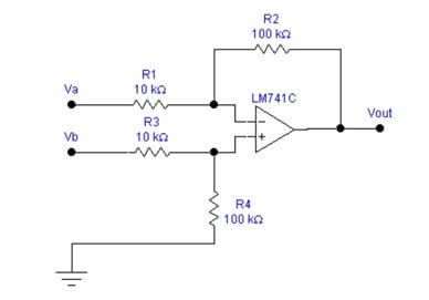
We will examine the op-amp version of the differential amplifier. You will appreciate the relative simplicity of the op-amp version. You may also observe that this amplifier is actually a combination of the inverting and non-inverting amplifiers.
An image of your Tinkercad circuit is required (please insert in the correct position in the report) for each measurement section.
Note: Some parts produce a perfect result, as expected from a simulation software. In practice, a difference is expected.
THE EXPERIMENT

1. Setup the power supply to have ±10V dual voltage outputs.
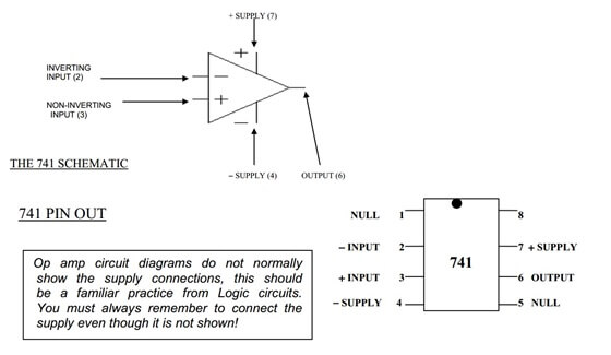
2. Construct the circuit shown below; pay special attention to the ±10V voltage and the ground connections from power supply. Label the pin numbers to make your connection process clear.

3. By the Superposition Theorem, we can measure the voltage output produced by a single input signal at a time; and the total output voltage will be the algebraic sum of each individual output voltage (or gain).
4. Measure the differential voltage gain Ava using superposition as follows:
a. Ground Vb;
b. Use the signal generator to generate the following signal and connect it to Va:
- Type of the signal: Sine waveform
- Frequency: f = 1kHz;
- Peak amplitude (Peak value): 5V
- Offset DC voltage: 0V.
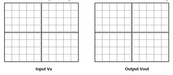
Use the oscilloscope to observe input Va on channel 1 and output Vout on channel
Sketch the signal voltages observed on the oscilloscope in the following:

c. From the waveform on scope, find the peak-to-peak values of the signals on input and output, respectively:
Va(PP) =
Vout(PP) =
d. Please circle the correct answer: the phase relationship between Va and Vout is:
- Out of phase or
- In phase
e. Calculate the voltage gain AVA based on your measurement (show your calculation procedures):
AVA =
5. Don’t change the setting of the signal generator, repeat step 4 but this time with Va grounded and apply the input signal to Vb. Record the peak-to-peak value of the signal and calculate the voltage gain AVB(show your calculation procedures):
Vb(PP) =
Vout(PP)
AVB =
6. Calculate the Average of the absolute value of the voltage gain AVA and AVB in step 4 and 5 and record it below (show your calculation procedures):
AAVG(D) =
7. Now we can measure the common mode gain Acm as follows:
- Short Va and Vb together.
- Apply a large 1kHz sine wave to both Va and Vb (e.g., 5Vpeak) together.
- Measure VOUT carefully and determine the common mode gain Acm (show your calculations), it should be <<<1. (You may see some noise in the output, just record the RMS value of the input/output and calculate the Acm)
Va(RMS) =
Vout(RMS)
Acm =
8. Calculate the COMMON MODE REJECTION RATIO (CMRR) in dB:
CMRR = 20log(AAVG(D)/ACM)
9. The highest CMRR results will be reached when the resistors are perfectly matched. For the poorly matched resistors, the results could be very different. To illustrate the effect of poorly matched resistors, change your resistors R3 and R4 as follows (leave R1 and R2 untouched):
R3= 12KΩ R4= 82KΩ
10. Repeat the measurements above and then determine the CMRR in dB:
Average AAVG(D) =
Acm =
CMRR in dB =
11. Compare results in step 10 and step 7, did you see any difference in Acm and CMRR?
QUESTIONS
- Use the theory you have learned from class, derive the output voltage Vout in terms of Va and Vb, assume R1=R3=10kΩ and R2=R4=100kΩ (Hint: You need to find the equation based on “virtual short”).
- Repeat question a) when R1= 10KΩ, R2= 100KΩ, R3= 18KΩ and R4= 82KΩ.


